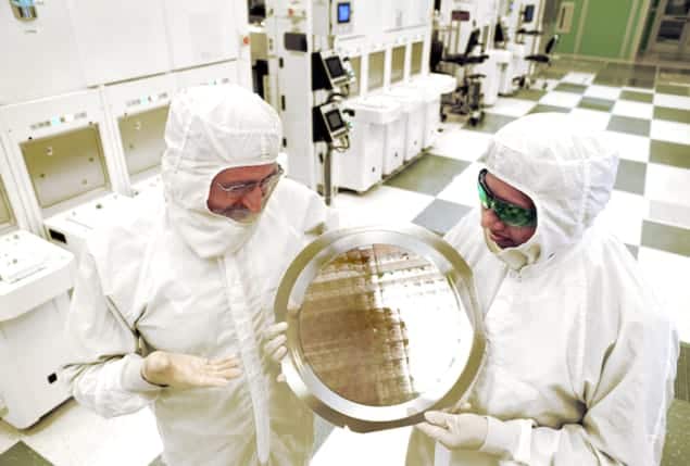
Scientists at IBM Research have made the first working prototype computer chips with circuit features as small as 7 nm. The milestone was achieved in collaboration with GlobalFoundries, Samsung and researchers at the SUNY Polytechnic Institute Colleges of Nanoscale Science and Engineering. Key features of the chips were made using silicon-germanium, rather than conventional silicon. The new technology could soon make it possible to pack 20 billion transistors onto a single chip – twice as many as is possible today.
In 1965 Gordon Moore, the co-founder of Intel, predicted that the number of transistors per unit area on integrated circuits would double every year, and this concept came to be known as Moore’s Law. The silicon industry has succeeded in following this law until quite recently, and this has given us myriad low-cost consumer electronics. Today, the smallest features on commercial chips measure 14 nm across, and some progress has been made on 10 nm and 7 nm devices. However, using conventional silicon-processing techniques to create working chips with features smaller than 10 nm requires several significant technological challenges to be overcome.
Bypassing convention
Now, the IBM-led collaboration has eschewed conventional semiconductor-manufacturing processes to create the first prototype 7 nm chip. The transistors used in the device are called “FinFETs” – complex devices that incorporate two gates. The transistor channels of the device – the parts that conduct electricity – are made from silicon-germanium (SiGe), rather than pure silicon. SiGe has higher electron mobility than pure silicon, which means that it is better suited for making tiny transistors.
The researchers have also managed to make use of very short wavelengths of ultraviolet light – extreme ultraviolet light (EUV) – to improve the lithography process for etching their tiny devices. EUV lithography can create much thinner lines than conventional techniques that rely on longer-wavelength light, although the etching rate is slower for EUV.
IBM also says that it used an “innovative” process to place the transistors closer together on a chip. Indeed, the devices boast a 30 nm pitch, which is the distance between the front edge of one transistor and the front edge of it neighbour.
Extending mainstream technologies
Mukesh Khare, vice president for semiconductor research at IBM, says that his company “has committed to spending $3bn on chip research and development aimed at further extending today’s mainstream semiconductor technologies”. He adds that IBM is also looking into materials other than silicon as the primary material in semiconductors and the use of transistors for processing data.
Stephen Chou, head of the NanoStructure Laboratory at Princeton University who was not involved in this work, says the 7 nm technology is a “significant step” for the integrated-circuit industry – in terms of both scaling and manufacturing. “Although my group fabricated the world’s smallest working individual silicon [transistors] (as small as 7 nm – in both length and width) in 1996, making [transistors] with similar dimensions on the industrial scale is extremely challenging and requires many innovations and billions of dollars of investment,” he says.
- This article first appeared on nanotechweb.org


