A new technique for directly growing diamond layers in selected areas on technologically relevant substrates could help remove heat precisely where it is needed in electronic devices, improving their performance. The scalable technique, which relies on microwave plasma chemical vapour deposition, can create diamond patterns on silicon and gallium nitride across length scales ranging from microns to full 2-inch wafers.
Unwanted heat is a major problem in electronics, and the issue only gets worse as devices become smaller. Synthetic polycrystalline diamond could come into its own here, thanks to the material’s high thermal conductivity, which allows it to efficiently dissipate heat. The problem, however, is that diamond is very hard and chemically resistant. This makes it difficult to shape using the conventional “top-down” techniques employed to carve fully-grown diamond layers to the sizes required.
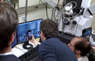
In the new work, a team of researchers led by materials scientists Xiang Zhang and Pulickel Ajayan and electrical and computer engineer Yuji Zhao of Rice University in the US turned to a bottom-up approach in which they build up diamond layer-by-layer using a plasma chemical vapour deposition technique. Their process, which is detailed in Applied Physics Letters, involves using microwave energy to ionize methane gas (CH4) so that it breaks down into its constituent carbon and hydrogen atoms. The carbon atoms then settle onto the substrate and assemble via a process that begins with nucleation. “Here, individual carbon atoms act as ‘seeds’ that other carbon atoms can latch on to,” explains Zhao.
Under these conditions, the researchers are able to control the thickness of the diamond by varying the growth time.
Controlling the seed location
To control the precise location of the carbon seeds, the team employed two techniques. The first was photolithography – a routine method in microelectronics that involves passing a light beam through a transmission mask to project an image of the mask’s light-absorption pattern onto a (usually silicon) wafer. The wafer itself is covered with a photosensitive polymer called a resist. Changing the intensity of the light leads to different exposure levels in the resist-covered material, making it possible to create small, finely detailed structures.
The approach, explains Zhao, is akin to using light to create a precise stencil, with the resulting structure acting as a mould for the diamond seeds. “Once the substrate wafers have been prepped, we spread a liquid containing nanodiamonds over their surface. These tiny specks then act as the starters for the diamond growth.”
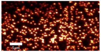
The particle size of the nanodiamond seeds was 5–10 nm, which ensured a high nucleation density (estimated to be around 1011–1012 cm-2) for subsequent diamond growth, Zhao adds. High-magnification scanning electron microscopy revealed that the diamond films consisted of densely packed grains that were smaller than a micron and that the patterned diamond films were around 2.5–3.5 µm thick. Raman spectroscopy confirmed that a diamond film had formed across the entire patterned region and that it was highly crystalline.
To prove how versatile this approach was, the team decided to selectively fabricate complex geometries – for example, a diamond structure in the shape of an owl, which is the mascot of Rice University – on a gallium nitride substrate.
A different technique for larger wafers
This technique worked well for small-area patterns, but for larger wafers, a different approach was required, explains Zhao. Instead of conventional photoresist lithography, the team laminated a commercially available lapping film onto a silicon wafer that served as a removable masking layer. A standard laser cutter was then used to define the boundaries of the desired pattern by selectively cutting through the film.
Next, the engraved regions were peeled off, exposing the underlying substrate only in the predefined areas. “We then carried out nanodiamond seeding by spin-coating a nanodiamond suspension over the entire wafer,” says Zhao. “After solvent evaporation, we mechanically lifted off the remaining lapping film, removing the nanodiamond seeds from the masked regions to leave a patterned seed layer on the exposed substrate that diamond can then grow on.”
This approach allowed the researchers to scale up to a full 2-inch wafer.
“The key result is that we can grow diamond on selected, predefined areas on technologically relevant substrates,” Zhao tells Physics World. “This will allow diamond – the best bulk thermal conductor known – to be placed precisely where heat removal is needed in a device, making practical integration much more feasible. Indeed, we showed that our films when employed as heat spreaders on a silicon substrate can reduce the operating temperature by more than 23 °C compared to bare silicon.”
Metallic material breaks 100-year thermal conductivity record

The team also discovered that smaller diamond islands were better at dissipating heat than a continuous diamond coating. “We found that the 50-micron diamond patterns achieved the most effective cooling because of their higher perimeter-to-area ratio,” Zhang explains. “These geometric features increase the density of the edge regions and help the heat dissipate more efficiently in three dimensions down into the silicon substrate.”
Thermal management is now a universal challenge – and is needed everywhere from AI GPUs and advanced logic (for example, FinFET technologies) to power electronics and photonics, Zhang adds. “As the global demand for AI accelerates, the associated power consumption and heat generation are becoming critical limits. Selective diamond integration offers a pathway to more efficient heat spreading across a broad range of technologies.”
Looking ahead, the researchers say they will now be working on direct device-level integration and making quantitative thermal measurements. They will also further optimize the material quality and interface engineering.