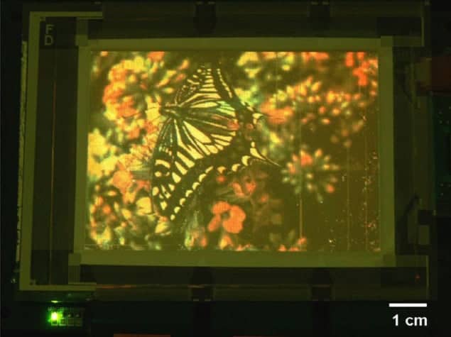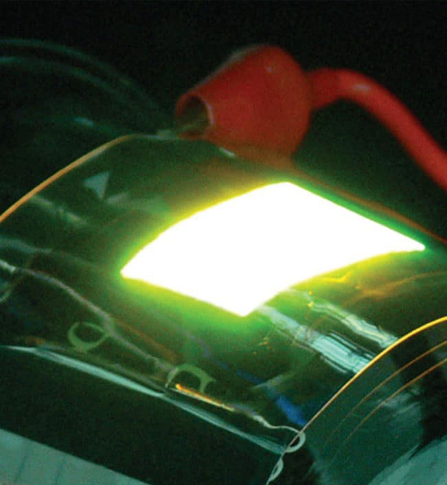
Researchers in South Korea and the UK say that they have produced the first large-area, full-colour display based on red, green and blue quantum dots. The technology could spur the launch of colour TV screens combining a vast colour range with an incredibly small pixel size.
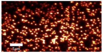
Both attributes stem from the intrinsic properties of the quantum dots, which despite being just a few nanometres in diameter comprise several thousand atoms that form tiny compound-semiconductor crystals. When electrons inside the quantum dots recombine with their positively charged counterparts, known as holes, it can result in the emission of a narrow band of light.
Making a colour display with the dots requires their deposition onto a substrate in a well-controlled manner. Monochrome displays can be made by spin-coating – dropping a dot-containing solution onto a substrate and spinning this around to yield a thin film of material. This approach is unsuitable for making a full-colour display, however, because it would cross-contaminate red, green and blue pixels.
Patterned rubber stamps
In this new work, a team led by Tae-Ho Kim at the Samsung Advanced Institute of Technology in South Korea, overcame this issue by spin-coating red, green and blue dots onto separate “donor” substrates, before transferring them in turn to the display with a patterned rubber stamp.
To make a 4-inch diameter, 320 × 240 pixel display, a pair of electron-transporting polymers was deposited onto a piece of glass coated in indium tin oxide. Red, green and blue dots were stamped onto this structure, which was then coated in titanium dioxide, a material with good hole-transporting properties.
Adding a thin-film transistor array allowed a different voltage to be applied to each of the 46 × 96 µm pixels. Increasing this voltage increases the brightness of the pixel, because more electrons and holes are driven into the dots, where they recombine to emit light.
Higher-resolution displays could be possible by reducing pixel size. “We showed an array of narrow quantum dot stripes of 400 nm width [in our paper], which indicates the feasibility of nano-printing quantum dots with extremely high resolution,” says Byoung Lyong Choi, one of the Samsung researchers. This demonstrates that the Korean team’s technology is more than capable of producing the displays with the highest practical resolution for viewing with the naked eye, which can resolve pixel sizes of up to 50 µm.
Improving efficiencies
One downside of the Korean display is its low efficiency – just a few lumens per watt, which is roughly half that of an incandescent bulb. But Choi says that far higher efficiencies should be possible by modifying their quantum dots. Samsung will continue to develop the technology, which it is trying to patent, before deciding whether to manufacture displays with this approach. “Transfer-printing can be scaled up to roll-to-roll systems for huge size printing onto flat or curved surfaces, such as rolled plastic sheets,” explains Choi.
John Rogers, a researcher at the University of Illinois, Urbana Champaign, is very impressed by the Korean effort: “It is, by far, the most complete demonstration of this technology.” However, Rogers also believes that the technology will face stiff opposition in the commercial market. “The entrenched technology – backlit liquid-crystal displays – continues to get better and better, and cheaper and cheaper.”
The Korean team reports its work in the latest edition of Nature Photonics.


