Researchers in the US have used electron microscopy to record detailed images of individual atoms. Philip Batson of the IBM Thomas J Watson Research Center in New York and Ondrej Krivanek and Niklas Dellby from Nion R&D in Kirkland, Washington, have observed individual gold atoms on a carbon substrate by using software to correct the image aberration that occurs in electron microscopes. Their work could have important applications in materials physics and biology, including the ability to image atomic impurities in semiconductors (P Batson et al 2002 Nature 418 617).

The resolution of electron microscopes is superior to that of optical microscopes because high-energy electrons have a much shorter wavelength than light. In the 1970s Albert Crewe at Chicago University and colleagues invented the scanning transmission electron microscope, which builds up an image by scanning an electron beam across a sample and measuring the electrons that are reflected and emitted back from the sample. Crewe’s team successfully imaged single uranium atoms with the device.
Researchers have since improved on this technique, but the blurring – or aberration – of magnetic lenses has limited the resolution of electron microscopes to about 50 times the wavelength of the electrons used. For electrons with energies between 100 and 200 keV, this resolution is about 0.2 nm, which is slightly larger than the typical distance between atoms.
Now Batson and colleagues have reduced this figure to less than 0.1 nm by using electrons with energies of 120 keV – electrons with energies greater than this cannot be used because they would damage the material under study. This means that the resolution of the electron beam is good enough to investigate the environment of individual atoms.
“This advance means that the electron probe is smaller than the inter-atomic distances,” says Batson. “We can now look into the bulk of a material to locate atoms which might be out of place or which might be of the wrong kind.”
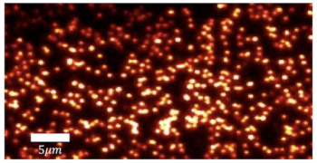
Batson and co-workers used a television camera to record ‘electron shadow images’ from a scanning transmission electron microscope and analysed these images with computer software to calculate – and correct for – the aberration of the microscope’s lenses. Using this arrangement they imaged gold atoms on a carbon substrate, observing single atoms and groups of atoms, both stationary and in motion. The IBM-Nion R&D team also demonstrated the technique on an alloy of germanium and silicon (see figure). The researchers say that this technique could also be used to image individual dopant atoms in semiconductors.
Earlier this year, Paul Voyles of Bell Labs and colleagues used an electron microscope to observe dopant atoms, but the resolution of their microscope – 0.16 nm – exceeded the inter-atomic distance in their sample.
“We believe aberration-correction technology combined with the inherent power of scanning transmission electron microscopes opens the way for smaller and smarter instruments to image and analyse materials at sub-0.1 nm resolution,” says Batson.
Correction: The original caption for the figure in this article was incorrect and was corrected on 27 September 2002.