Physicists in the US have made quantum dots in graphene by simply introducing strain into the material. By creating tiny structures in which graphene is stretched like a drumhead, researchers say they are the first to show that charge carriers can be confined within the material by straining it. The results of this latest work could help in the development of graphene-based electronic devices such as transistors and optoelectronics components.
Graphene – a honeycombed lattice of carbon just one atom thick – is an excellent conductor of electricity thanks to the fact that electrons can whizz through the material at extremely high speeds with little resistance. This means that the material could one day be used to make transistors that are faster than any that exist today. However, graphene’s extreme conductivity is also a problem, because electronic devices made from the material cannot be effectively switched off. This not only wastes power, but also means that such devices cannot be packed onto computer chips in the same way that silicon components are today.
Lack of band gap
Although graphene is a type of semiconductor, it is unlike familiar materials such as silicon because it does not have an energy gap between its valence and conduction bands. Such a band gap allows a semiconductor to switch the flow of electrons on and off. Researchers have proposed various schemes to overcome this problem – for example cutting graphene into nanoscale ribbons or dots, or chemically modifying the material to create a band gap. While these schemes work in principle, altering graphene in these ways also damages the material so much that finished devices no longer have the desired high electron mobility.
Now, Joseph Stroscio of NIST in Gaithersburg, Maryland, and colleagues have modified the electrical properties in graphene simply by stretching the material. The researchers say that distorting graphene appears to have the same effect as applying a strong magnetic field and can produce quantum dots in the material. Quantum dots are tiny semiconducting structures in which electrons are confined in all three dimensions. It is this confinement that gives quantum dots unique electronic and optoelectronic characteristics, which can often be fine-tuned by adjusting the size of the structure. The ability to create semiconducting regions in graphene in this way might offer a way of making devices that offer both high electron mobility and a band gap.
Graphene “drumheads”
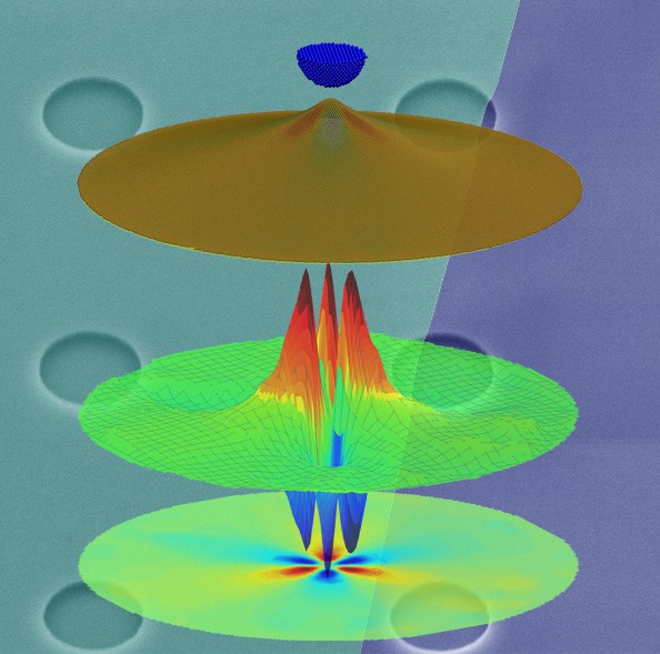
Stroscio’s team did its experiments on graphene “drumheads”. These were made by placing graphene flakes over a series of holes (each about 1 µm across) that was deeply etched in a silicon-dioxide wafer. The technique is rather like placing a sheet of plastic clingfilm over a tiny muffin tin. The silicon dioxide is an insulator and beneath it is a layer of conducting silicon, which acts as a gate electrode when a voltage is applied between it and the graphene.
The researchers then strained the graphene by pulling it up and away from the silicon dioxide with the attractive force from the tip of a scanning tunnelling microscope (STM). At the same time, the graphene was also pulled down using the electrostatic force from the silicon gate. Careful adjustment of the opposing forces allowed the team to have very precise control over the shape of the graphene drumheads, explains Stroscio.
Fictitious magnetic field
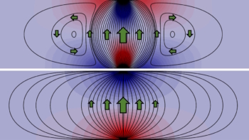
When the graphene is stretched or strained in this way, charge carriers (electrons and holes) in the material begin to move in circles rather than simply travelling in straight lines, as is usually the case. “Mathematically, the applied strain can be likened to a fictitious magnetic field,” says Stroscio, “and this field makes the charges travel in circles, just as they would in a real magnetic field.”
According to calculations performed by the researchers, the graphene drumhead is strained in the region around the STM probe tip, which produces a shape that looks like a circus tent as it pulls up the graphene sheet. The charge carriers are thus confined around the apex of the tent, in the same way as they would be confined in a quantum dot.
“Our experiments are the first to show that strained graphene confines charge carriers like in a quantum dot,” Stroscio told physicsworld.com. “Normally, you would have to cut out a nanosized piece of graphene to make a quantum dot out of the material, but our work shows that you can achieve the same thing with strain-induced pseudo-magnetic fields.”
The team, which includes scientists from the University of Maryland in the US and the Korea Research Institute of Standards and Science in Seoul, is now performing more comprehensive simulations to find out whether the size of the quantum dots in graphene can be tuned. “We are also busy looking at how intense the fictitious magnetic fields can become, and engineering different strain fields in graphene,” reveals Stroscio.
The research is reported in Science.


