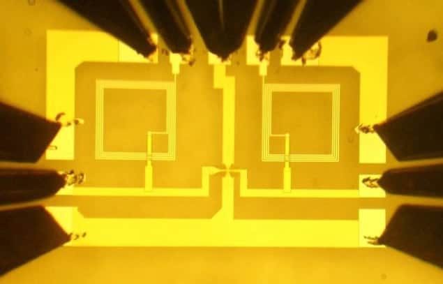
IBM researchers have made the first graphene circuit in which all of the circuit elements are integrated on a compact single chip. The new circuit is another important step forward for graphene-based electronics and potential applications include wireless communications and amplifiers.
Despite much progress in recent years and the fact that scientists have already made some high-performance graphene-based devices, it still remains challenging to integrate graphene transistors with other components on a single chip. This is mainly because graphene does not adhere very well to the metals and oxides traditionally used in semiconductor-manufacturing processes and because there are no reliable and reproducible techniques yet to make such circuits.
Integrated inductors
Now, Phaedon Avouris and colleagues at IBM’s T J Watson Research Center in Yorktown Heights, New York, may have overcome this problem with their new integrated circuit that consists of a graphene transistor and a pair of inductors compactly integrated on a silicon carbide (SiC) wafer. The wafer-scale fabrication process the team developed is compatible with conventional semiconductor-fabrication methods and can be used to produce circuits in high yields.
The researchers synthesized their graphene by thermal desorption of silicon from SiC wafers to form uniform graphene layers on the insulating SiC surface. They then defined the transistor channel using electron-beam lithography, removing graphene outside of channel regions with an oxygen plasma. Inductors were defined by electron-beam lithography and formed by depositing micron-thick aluminium metal onto the wafers. Finally, a 120 nm thick layer of silicon dioxide, deposited by electron-beam evaporation, was used to isolate the inductor loops from the underlying metal interconnects.
The circuits operate as radio-frequency “mixers” up to 10 GHz, says team member Yu-ming Lin. As the name suggests, mixers produce output signals with mixed frequencies and are fundamental components of many electronic communications systems. In their device, the researchers apply two high-frequency signals to the gate and the drain of the graphene circuit. The graphene transistor is modulated by both signals and produces a drain current that contains the mixed frequencies.
Wireless communications
“The circuit, as it stands, could already be used for wireless communications,” Lin told physicsworld.com. “And by further optimizing the performance of the graphene transistors, it might be used as an amplifier.”
The importance of the work goes beyond the actual circuit demonstrated and other circuits can be made using the same technique, he adds. It could also be applied to different types of graphene materials, including chemical vapour deposited (CVD) graphene films created on metal films. Most importantly, it could be used on silicon and other semiconductors to form hybrid circuits with new functionalities.
The team is now busy working on improving the performance of the transistors by optimizing device structure, graphene quality and the gate dielectric. “We are also developing more complex graphene circuits for even more sophisticated devices,” says Lin.
The work is detailed in Science 332 1294.


