Since its discovery in 2004, graphene continues to fascinate physicists with its growing list of exceptional electronic and mechanical properties. While small pieces of the material — which is a sheet of carbon just one atom thick — are easy to make, it has proven more difficult to make large-area, high-quality samples that could be used in graphene-based devices.
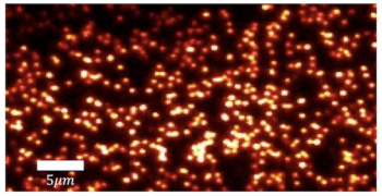
Now researchers in France may have come up with a simple way of making relatively large pieces of graphene. Abhay Shukla and colleagues of Pierre and Marie University in Paris show that bulk graphite can be bonded onto borosilicate glass and then cleaved off to leave a single layer of graphene on the substrate.
The most common “peeling-off” method to produce graphene is only useful for making small-scale prototype devices but the new method makes it possible to apply this approach on a larger scale while preserving high sample quality, says Shukla.
Sticking to glass
The researchers used a technique known as anodic bonding, which sticks a conductor or semiconductor onto a glass substrate using large electrostatic forces that come from the ionic conductivity of the substrate. This means that no adhesive is required. The method is widely used in the microelectronics industry to bond silicon wafers to glass.
“This technique had never been tried on layered substances, like graphene, presumably because they do not stick but peel off, but we turned this phenomenon to our advantage” explained Shukla. “Only the first or first few atomic layers remain bonded to the substrate while the bulk can be peeled off.”
Because the samples are bonded to a rigid glass substrate, this produces larger surface area samples of high quality in an efficient and simple way. The method might be used for other layered materials as well.
So far, the researchers have produced millimetre-sized samples but say that they could improve on this. “Materials other than graphene will produce bigger samples still, making possible applications in microelectronics and fundamental experiments limited by sample size,” said Shukla.
Suspended atomic layers
The team would now like to extend the method to other substrates. It would also like to use appropriately micropatterned substrates to make suspended atomic layers.
Shukla says that he already uses the technique for making X-ray mirrors by bonding single crystal silicon onto glass substrates for use in X-ray spectrometers at synchrotrons. “When I heard of graphene, I immediately thought of trying to use the method for making this material.”
The work was reported in Solid State Communications.