Physicists in the US have made the fastest graphene transistor ever, with a cut-off frequency of 100 GHz. The device can be further miniaturized and optimized so that it could soon outperform conventional devices made from silicon, says the team. The transistor could find application in microwave communications and imaging systems.
Graphene – a sheet of carbon just one atom thick – shows great promise for use in electronic devices because electrons can move through it at extremely high speeds. This is because they behave like relativistic particles with no rest mass. This, and other unusual physical and mechanical properties, means that the “wonder material” could replace silicon as the electronic material of choice and might be used to make faster transistors than any that exist today.
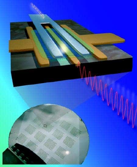
Phaedon Avouris, Yu-Ming Lin and colleagues at IBM’s TJ Watson Research Center in New York began making their field-effect transistor (FET) by heating a wafer of silicon carbide (SiC) to create a surface layer of carbon atoms in the form of graphene. Parallel source and drain electrodes were then deposited on the graphene, leaving channels of exposed graphene between them.
Protecting the graphene
The next step is the trickiest – depositing a thin insulating layer onto the exposed graphene without adversely affecting its electronic properties. To do this, the team first laid down a 10 nm layer of poly-hydroxystyrene – a polymer used in commercial semiconductor processing – to protect the graphene. Then a conventional oxide layer was deposited, followed by a metallic gate electrode.
The gate length is relatively large at 240 nm, but it could be scaled down in the future to further improve device performance, say the physicists.
The graphene transistor already has a higher cut-off frequency than the best silicon MOSFETs with the same gate length (these have a cut-off frequency of around 40 GHz). The cut-off frequency is the frequency above which a transistor suffers significant degradation of its performance. The new device breaks IBM’s previous record of 26 GHz, reported on in January 2009.
‘Technologically relevant’
Unlike most other graphene FETs, which have been made from flakes of graphene, this device is made using techniques used by the semiconductor industry. “Our work is the first demonstration that high-performance graphene-based devices can be fabricated on a technologically relevant wafer scale,” Avouris said.
One shortcoming of such graphene devices, however, is that they cannot be used in digital circuits such as those found in computers. This is because graphene has zero energy gap between its conduction and valence electrons – and it is this “band gap” that allows conventional semiconductors to switch currents from off to on.
Instead, such high-frequency transistors could be used to amplify analogue microwave signals in communications and imaging applications – including high-resolution radar, medical and security imaging.
The IBM researchers now plan to scale down their transistor, improve graphene purity and optimize device architecture. “Such transistors could then far outperform conventional devices,” said Avouris.
The team is also looking at ways of creating a bandgap in a graphene transistor so that it could be used in digital applications.
The result was published in Science.


