Flat, high-efficiency, ultrathin metasurface lenses, that focus light to subwavelength spots, have been developed by researchers in the US and Canada. The devices – which produce images comparable to top commercial lenses – were manufactured in an industrially viable way and could be used in laser-related imaging, microscopy and spectroscopy. They could be further developed for use in mobile-phone cameras and wearable electronics.
In optics, Fermat’s principle governs the operation of lenses, and states that light follows the path along which it accumulates the least phase. It bends towards the normal in regions of higher refractive index, to travel a smaller distance where the wavelength is shorter and phase accumulates more quickly. Phase accumulates continuously as the wave propagates, so the lens requires a finite thickness for waves to accumulate enough phase to be redirected as desired.
Discontinuous redirection
In 2011, however, Federico Capasso and colleagues at Harvard University showed that, if the phase of light waves could be changed discontinuously, the light could be redirected as desired using a flat surface. In their original work, this was achieved using resonant metallic antennas that interfered directly with the electric field of the light. But the antennae were difficult to manufacture and highly inefficient.
Researchers have since shown that phase discontinuities can also be imprinted by using tiny subwavelength elements made of silicon. These imprint a shift in the so-called Pancharatname–Berry phase of the light waves, by imparting a spatially dependent polarization shift as they pass through the elements. These elements are simpler to manufacture and focus transmitted visible light more efficiently, but they still absorb or reflect too much light to make a viable commercial lens.
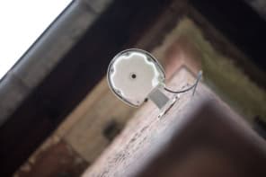
Capasso’s team has now developed a new technique to fabricate these tiny “nanofins”, using electron beam lithography to pattern a resist before depositing a very thin layer of titanium oxide – which transmits visible wavelengths much better than silicon – onto the resist to produce the metasurface. The researchers used their technique to fabricate titanium-oxide metalenses designed to focus light at different visible wavelengths.
Titanium nanofins
The focusing efficiencies of the lenses were unprecedented for visible-light metalenses: the lens designed for 405 nm (violet) light brought 86% of the incident light to a focus. The lenses also had much higher numerical apertures than previous metalenses, allowing them to focus light from a wider angle to a single spot. This in turn produced focal spots smaller than the light’s wavelength, and smaller than those achievable with a state-of-the-art commercial objective containing multiple refractive lenses.
The researchers also demonstrated imaging with the metalenses for the first time in the visible region, showing that they could produce highly magnified images of several different test objects and resolve features less than one wavelength apart. The team’s lenses do suffer from quite large chromatic aberration – while this is not a problem for technical applications such as microscopy performed with monochromatic laser light, it would be for consumer applications such as camera lenses. Luckily, in 2015, Capasso and colleagues showed that a strategically designed silicon metasurface could focus multiple infrared wavelengths at the same point, and Capasso believes this should be possible at visible wavelengths too. “It’s just a matter of time before we do it also with titanium oxide,” he says. “With our lens, we believe that we can replace the ordinary lens in lots of cameras to make things more compact, cheaper, thinner and achieve the same performance.”
Andrea Alù of the University of Texas at Austin, who was not involved in the research, is impressed. “We have seen this series of papers in the last few years on metasurfaces, and the question has always been, ‘What is the efficiency? Can we ever make this competitive with known optical components? ” he told physicsworld.com. “This paper addresses some of these questions: it says that we can indeed build large-area metasurfaces that are still very thin, they are dielectric – so low loss – and yet they can provide a large numerical aperture, and goes forward to compare the response with state-of-the-art commercially available components.”
He points out, however, that the Pancharatmane–Berry phase shift is inherently polarization dependent, and that Capasso’s efficiency measurements were made using appropriately polarized light. “You cannot just put this on an iPhone camera and expect it to work for ambient light,” he explains. “I guess you could put in filters, but that sacrifices efficiency.”
The research is published in Science.