A skin-like sensor array that can convert touch directly into light signals has been built from individual-nanowire light-emitting diodes by researchers in the US. The new device appears to be more sensitive to touch than even human skin. It might be ideal in robotics applications, in next-generation touchscreen pads, for improved human–machine interfaces, biological imaging and optical microelectromechanical systems (MEMS), to name but a few.
Unlike the other four human senses – vision, hearing, smell and taste – touch remains stubbornly difficult to mimic in the laboratory. A good artificial skin needs to be highly sensitive to touch over areas at least as small as 50 microns and respond quickly to applied pressure. Researchers have already succeeded in making sensor arrays for such electronic skin, or “e-skin”, from assembled nanowires or microstructured rubber layers that change their capacitance or resistance in response to pressure or force. But these materials are only able to map applied strain distribution at resolutions of millimetres, at best.
A team led by Zhong Lin Wang at the Georgia Institute of Technology may now have gone a long way in resolving this problem by developing the first individual LED-based pressure/force sensor array for fast mapping of strain at distances smaller than just three microns. The pixel density of the new device is also extremely high at 6350 dots per inch (dpi), which is a 1000 times better than the previous record for such sensors. Each pixel is made up of a LED comprising single zinc-oxide nanowires grown atop p-doped gallium nitride and is sensitive to locally applied pressure, force and strain thanks to the so-called piezophototronic effect.
Piezoelectric potentials
Piezoelectric materials produce a polarization charge when subjected to mechanical strain, as the symmetry of the component crystals becomes distorted. Piezophototronic devices rely on this principle to control electron transport and recombination by the polarization charges present at the ends of individual nanostructures adjacent to the p–n junction, where the light is generated. In the new work, the strained zinc-oxide nanowires create a piezoelectric charge at both their ends, which forms a piezoelectric potential, explains Wang. This potential distorts the band structures in the wire, which allows electrons to remain in the region of the p–n junction longer and so enhances the LED’s light-emitting efficiency.
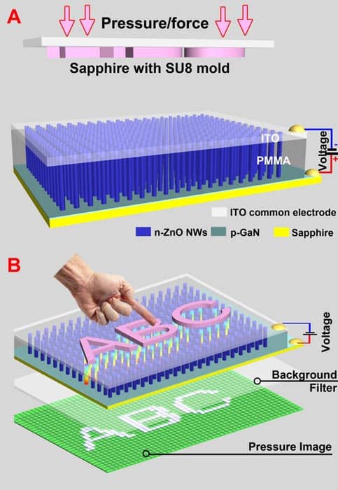
The light output from the device varies with applied pressure. This output signal is electroluminescence light that can easily be integrated with on-chip photonic technologies for fast data transmission, processing and recording. And instead of using conventional “cross-bar” electrodes for sequential data output, the pressure image or map is received in parallel for all of the pixels, says Wang. This means that the output signal can be detected much faster (in just 90 milliseconds) than in the traditional designs based on piezo-resistance or -capacitance effects.
“This approach may be a major step towards digital imaging of mechanical signals by optical means with potential applications in touchpad technologies, personalized signatures, bio-imaging and optical MEMS,” Wang told physicsworld.com. “Such sensor arrays could also be fabricated on flexible substrates (such as PDMS or carbon fibres) since patterned zinc-oxide nanowires can be grown on any surface using low-temperature solution-based growth methods, something that could open up a host of other application areas.”
The team made its devices using a low-temperature chemical growth technique to create patterned arrays of zinc-oxide nanowires on a gallium-nitride thin-film substrate. The researchers then flooded the spaces between the nanowires with a PMMA thermoplastic and used an oxygen plasma to etch away enough of the PMMA to expose the tops of wires. The final steps consisted of forming an ohmic contact with the underlying gallium-nitride film using a nickel–gold electrode and depositing a transparent indium-tin-oxide film on top of the array as the common electrode.
More sensitive robots and better prosthetics?
The sensor arrays can detect pressure changes as small as 10 KPa, which is similar to a gentle finger tap. In addition to possibly providing robots with a more sensitive sense of touch, which would allow them to adjust the force they use to grasp things, the new devices might also come in handy for improving human prosthetics. They might even be used to improve something called electronic-signature mapping. Here, the sensors would record the pressure or force applied when a person signs their name, as well as the speed with which they write, to make signatures much more secure.
The team says that it will now be looking at how to improve the spatial resolution of the arrays even further. This might be done by reducing the diameter of the nanowires so that many more can be fitted onto an individual array and by using higher-temperature fabrication processes.
The research is published in Nature Photonics.