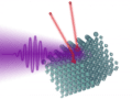
A photoelectric system that converts light into charge and then stores the charge like a battery – a first for a single device – has been developed by researchers in China and Singapore. Made from layers of a 2D semiconductor and a transparent conductor held together by weak van der Waals interactions, the new device converts 93.8% of incident photons into electric current – far higher than the 50% typical for so-called “high performance” photoelectric devices – and can store charge for up to a week, making it suitable for applications in energy generation, photodetectors or light-based memory.
Van der Waals (vdW) heterojunctions like the one used here are a common feature in devices such as photovoltaic cells and photodetectors. Often made from p-n junctions, they work by absorbing photons that then create electron-hole pairs. The next step is to separate the electrons from the holes, which is usually done by applying a voltage. The problem is that these charge carriers rapidly recombine, shortening their lifetime and therefore limiting the device’s external quantum efficiency (EQE).
Temporarily trapping the carriers
One way to overcome this effect is by temporarily trapping the carriers (at crystal defects, for instance) before recombination can occur. A team of researchers led by Yucheng Jiang of the Suzhou University of Science and Technology in China and Cheng-Wei Qiu of the the National University of Singapore decided to use this strategy in a vdW p-n heterojunction made from tungsten selenide (WSe2) and strontium titanium oxide, or STO as it is commonly known.
The team found that when they excited their device with blue laser light and then stored it in the dark at a temperature of 30 K, the photogenerated charge carriers persisted for as long as seven days. They also found that they could extract a current as large as 2.9 mA when they connected the device to a circuit. The researchers attribute this unexpected effect to a special treatment that produced a nearly two-dimensional “electron gas” on the surface of the STO, in which electrons can move freely and independently.
“Chargeable photoconductivity”
The researchers dubbed this new effect “chargeable photoconductivity”, and they say it is completely different to previously observed photoelectric phenomena. The device they made not only creates photocarriers under optical illumination but also stores them in the so-called “space-charge” region of the WSe2 film, which juxtaposes the interface with the STO crystal. Here, they explain, light-induced holes can accumulate and be retained until a sufficiently large applied voltage draws them into a circuit. During this process, the electron-hole pairs recombine and the device returns to the insulating state. It can then be charged anew by shining light on it.
How long does the photoelectric effect take?
Although the device’s EQE is much higher than that of other high-performance photoelectric devices, Jiang and colleagues note that it only achieves this efficiency at temperatures of around 30 K, which are required to keep the stored charge stable. This low operating temperature will limit the device’s applications, although the researchers believe the operating temperature might be increased by employing materials other than WSe2 and STO.
The researchers report their work in Physical Review Letters.