A new inkjet-based printing technique for making high-performance, single-crystal thin-film transistors has been developed by a team of researchers in Japan. The room-temperature process could be used to make large-area printed electronics, including flexible displays, solar cells, electronic paper and sensor sheets.
High-purity single crystals have been crucial in advancing semiconductor microelectronics, and devices with the highest performance invariably contain single-crystal interfaces. Printing techniques, such as inkjet technology, show promise for making large-area and flexible electronic devices and work by depositing patterns on a substrate using inks made of semiconductor materials. One major problem with inkjets is that the deposited materials have poor crystalline properties, which reduces charge-carrier mobility in the material and ultimately degrades device performance.
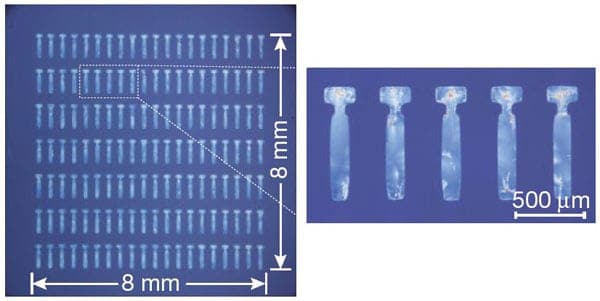
Now, Tatsuo Hasegawa of the National Institute of Advanced Industrial Science and Technology (AIST) in Tsukuba and colleagues have come up with a new printing process that combines a semiconductor ink and a crystallization ink into one. The first is a semiconductor in a solvent and the second, an “antisolvent” – a liquid in which the semiconductor is insoluble. The method produces exceptionally uniform, single-crystal or polycrystalline thin films that grow at the liquid–air interface on a substrate.
Avoiding ‘coffee rings’
“These results are strikingly different from those achieved with previous such printing methods,” Hasegawa tells nanotechweb.org. “Until now, it was difficult to produce uniform semiconducting thin films with [high-quality crystals] because of self-crystallization, or the ‘coffee-ring’ effect.” This effect involves the movement of tiny particles in a solvent that is driven by evaporation.
The team used a piezoelectric inkjet printing machine with double printing heads that eject droplets of 60 pl at a frequency of 500 Hz. During the process, the antisolvent ink (pure anhydrous dimethylformamide) is printed first and then overprinted with the ink containing the organic semiconductor C8BTBT. The deposited droplets then naturally mix together on the surface of the substrate.
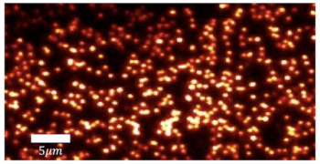
Using an optical microscope, the researchers observed tiny floating bodies that begin to form at the liquid surface. Each body seems to act as a nucleus for further crystallization and subsequently grows larger. These bodies eventually cover the entire surface of the droplet to form C8BTBT thin solid-like layers before the solvent evaporates. The solvent evaporates quite slowly, with the final result being films of C8BTBT that are around 30–200 nm thick, sticking tightly to the substrate surface.
High-performance mobility
The researchers used this material to make thin-film transistors with a gold source and drain electrodes and Parylene-C as the gate dielectric layer. The finished devices have average charge-carrier mobilities as high as 16.4 cm2/Vs. Such a value puts the devices into the high performance range, which starts at 10 cm2/Vs. The on-off current ratio is also high, at 105–107.
According to Hasegawa, this performance is much higher than previous transistors made from C8BTBT and compares well with other very-high-performance devices, including rubrene single-crystal devices. “We believe the good properties observed come thanks to the fact the single-crystal thin semiconductor film forms slowly. This is because of the fluid nature of the microliquid droplet in which laminar flow dominates over turbulent flow.” The technique should also work for other functional soluble materials, he adds.
The team, which includes researchers from the University of Tokyo and KEK in Tsukuba, now plans to optimize its equipment and device-processing techniques. “For example, there is plenty of scope for improving the source/drain contacts in our transistors,” reveals Hasegawa. “The next step will then be to exploit the technique for making printed electric metal wires and then ultimately produce all-printed electronic products.”
The work was published in Nature DOI:10.1038/nature10313.


