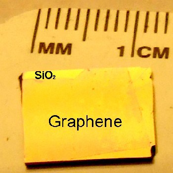
Researchers in Texas are the first to produce centimetre-sized samples of graphene — sheets of carbon one atom thick and dubbed the “wonder material” on account of its unique physical properties. This is significantly larger than existing samples that are typically at the micrometer scale. Richard Piner and his team at the Univeristy of Texas have employed a chemical deposition technique to grow their graphene on thin films of copper.
Graphene holds the promise of revolutionizing electronics over the coming years. One of the main reasons is that electrons travel through graphene with significantly higher mobility than they do in conventional circuits made from silicon. Engineers have already created some rudimentary graphene components, such as transistors and frequency multipliers. However, making carbon-based circuits will require large and high-quality samples of graphene that can be integrated with silicon.
Wondrous production
Since its discovery in 2004, there have been a range of approaches to isolating graphene from larger samples of carbon. One of the favoured techniques is mechanical exfoliation in which flakes of graphene are stripped from graphite with “sticky tape”. However, due to the delicacy of a material that is just one atom thick, exfoliation typically produces flakes at the nano-scale.
“They say a 30 cm graphene sample is the Holy Grail for carbon electronics but reaching the same order of magnitude is a significant step,” said Richard Piner, one of the researchers at the University of Texas.
Piner and his colleagues take a different approach by growing graphene on a substrate using chemical deposition. Taking a piece of copper foil 25 µm thick, they add a mixture of methane (CH4) and hydrogen, then heat the apparatus to 1000 degrees Celsius. Single layer graphene is then deposited on the copper in patches up to 1 cm by 1 cm.
Drop the copper
“This very important result may represent the missing link in the industrial fabrication of large area graphene for applications in graphene-based integrated electronics,” said Roman Sordan, a materials researcher at the Politecnico di Milano.
Previously, researchers had used chemical vaporization but with different metals and this have hindered the quality and scale of carbon growth. For example, nickel has been touted as promising, but carbon is highly soluble in this metal and multiple layers of graphene tend to build up at the grain boundaries.
Now that the team from Texas have produced a large sample of graphene, the next step is to develop a technique for carefully transferring the carbon sheet from the copper to a semiconductor — like silicon. Piner told physicworld.com that initial attempts have resulted in limited success. “We are working on the fact that graphene is extremely hydrophobic and can float to the surface of a liquid… but it is also extremely delicate,” he said.
This research was published in Science


