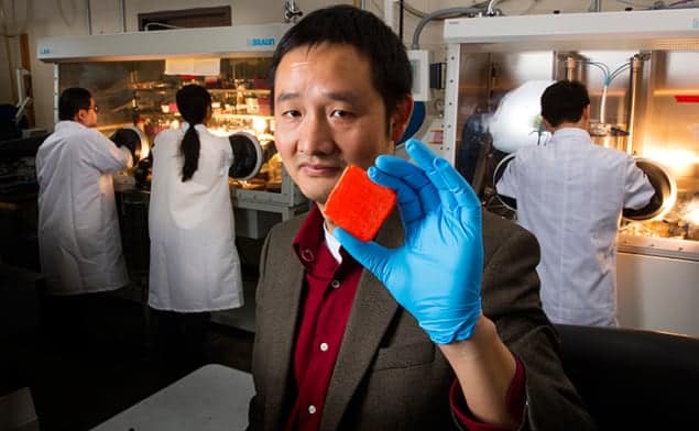
A new, highly sensitive X-ray detector that could be used for medical imaging has been built by researchers in the US, the Netherlands and China. The researchers anticipate that the detector will allow X-ray images to be taken using smaller doses of ionizing radiation, and therefore smaller cancer risks to the patient.
X-rays are immensely useful for medical diagnosis and treatment monitoring because they are highly penetrating, passing through skin and soft tissue to reveal bone and deep tissue. However, X-rays also pass easily through the materials used in detectors and this makes these devices inefficient. As a result, sophisticated diagnostic protocols such as computed-tomography (CT) scans involve relatively high doses of X-rays to acquire high-quality images – and such doses carry a known cancer risk. Reducing radiation dose by developing more sensitive X-ray detectors is therefore a very active field of research in medical physics.
When an X-ray photon passes through a semiconductor-based detector, it generates electron–hole pairs. A voltage applied across the detecting volume causes the electrons and positive holes to move in opposite directions. By measuring the resulting current, one can calculate the intensity of radiation striking the detector. Modern X-ray detectors normally use amorphous selenium as the detecting material. Jinsong Huang of the University of Nebraska–Lincoln says such devices are easy to manufacture at large scale and integrate into silicon circuits, but their sensitivity is limited by the selenium’s relatively low absorbance of X-rays.
Heavy metal
An atom’s X-ray absorbance is proportional to the fourth power of its atomic number (Z). Therefore, perovskite minerals containing the heavy metal lead (Z = 82) are extremely good absorbers. In 2015, Wolfgang Heiss of Johannes Kepler University Linz and colleagues unveiled an X-ray detector based on a solution-processed perovskite thin film. Unfortunately, the thickest films they could produce were only 60 μm thick – too thin to stop the high-energy X-rays used in medical imaging. Furthermore, these films were polycrystalline, which meant that the electrons and holes tended to recombine at grain boundaries. In the same year, however, several research groups developed techniques for producing single-crystalline thin perovskite films by solution processing.
In this latest research, Huang and colleagues used a modified version of one such technique to produce 2–3 mm-thick single-crystal X-ray detectors of the perovskite methylammonium lead tribromide. These have much higher charge mobilities and lifetimes than previous materials, which allows electrons and holes to be extracted with only a 100th of the applied voltage. This property is important because increasing the voltage also increases the “dark current”, which contaminates the signal.
The researchers say their new detectors are four times more sensitive than amorphous selenium detectors, and are therefore able to detect weaker X-ray signals. However, Huang explains that the detector is not yet sufficient for medical imaging because practical applications require an array of detectors rather than just a single device.
Ease of production
Heiss agrees that the technology must be expanded from a single detector to at least a linear array of detectors before it is suitable for medical applications. Heiss, who was not involved in the research, adds that the semiconductor physics done by Huang’s team is “significant”. The lifetimes and mobilities of the charge carriers, he says, are comparable with those of traditional semiconductor crystals grown by far more delicate and laborious methods. “They get the same quality, but in a much easier way,” he says, “which I think is something astonishing.” He reserves judgment, however, about the medical potential.
John Rowlands of the Sunnybrook Health Sciences Centre in Toronto, who helped develop the amorphous selenium detector, also praises the “excellent, interesting work”, although he too believes obstacles remain to its medical implementation. He says that relying on high charge mobility to obtain charge extraction at low voltage could compromise the resolution of a detector because charges would also drift laterally.
Rowlands also points out that, although the quality of the least exposed parts of the image would be improved, “maybe substantially”, one cannot assume that a smaller dose of X-rays could be used because an optimum number of photons are needed to smooth out their random fluctuations in the other parts of the image. Finally, he says that the parameters referenced in the paper for the quality of amorphous selenium detectors are taken from a paper published in 2000, and since then “amorphous selenium development has not stood still”.
The research is described in Nature Photonics.


