Scanning tunnelling microscopes (STMs) have been used for nearly three decades to study the surfaces of metals and semiconductors. But now physicists in Germany have discovered that the instruments can be used to measure the behaviour of electrons relatively deep within a material.
According to the researchers, the technique offers a completely new way of measuring the shape of the “Fermi surface” — the boundary between occupied and unoccupied electron energy states that defines many of properties of metals and semiconductors. And because STM can be sensitive to the spin of electrons, the technique could be used to characterize the tiny magnetic structures used in data storage devices.
An STM works by placing an extremely small metal tip (with just one atom at its point) very close the surface of interest. When a voltage is applied between tip and sample, electrons tunnel into or out of the material. The size of the tunnelling current is related to the surface properties of the material, such as mapping the locations of individual atoms.
Alexander Weismann and colleagues at the University of Goettingen, the Institute for Solid State Research in Juelich and the Martin Luther University in Halle made their discovery while developing an STM technique for locating atomic impurities below the surfaces of materials (Science 323 1190).
Colliding wavefronts
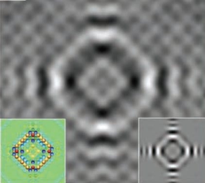
This involved studying samples of copper that contained minute quantities of cobalt. Electrons injected from the STM tip into pure copper should travel in wavefronts much like the ripples formed by a stone dropped in water. However, if such ripples encounter a cobalt atom they can be scattered back to the surface where they interfere to form a pattern that could be detected by the STM.
While the technique was able to locate the cobalt atoms, the team was surprised to see that the interference pattern was more complicated than expected from simple ripples. Instead, the pattern corresponded to the underlying symmetry of the copper crystalline lattice. The reason, according to the team, is that the ripples are being focused along certain directions in the copper — an effect that is defined by the shape of the Fermi surface.
Team member Martin Wenderoth at Goettingen told physicsworld.com that the technique is sensitive to the shape of the entire Fermi surface. By contrast, established techniques for measuring the Fermi surface, like electron cyclotron resonance and angle-resolved photoemission, map out only selected parts of it.
Wenderoth says that the technique could be used study local variations in the shape of the Fermi surface. For example, it could be used to study hidden interfaces in nanometre-sized multilayered structures.
Two Fermi surfaces
In particular, it could be very useful in characterizing layered magnetic structures such as those used in giant magnetoresistance (GMR) read heads for computer hard drives. This is because magnetic materials such as iron and cobalt have two different Fermi surfaces — one for spin up electrons and one for spin down electrons.
Spin-polarized STM, which is sensitive to the spin of the tunnelling electrons, would see two interference patterns if the electrons travelled through a magnetic layer — one for spin up electrons and the other for spin down. By observing the two different patterns, researchers could gain insight into the magnetic and structural properties of magnetic layers buried under a surface.


