It may seem that anything traditional materials can do 2D materials can do better, but when it comes to a resistive device you can switch on or off, leakage currents can pose problems when materials are atomically thin. Drawing on their expertise in high-quality monolayer device fabrication Jack C Lee and Deji Akinwande at the University of Texas at Austin Microelectronics Research Center in the US and their colleagues in the US and China have now demonstrated resistive switching across monolayer hexagonal boron nitride (h-BN) bringing the record thickness for a memory material down to around 0.33 nm.
Non-volatile resistance devices switch between high and low resistance states when a voltage is applied, a process described as setting and resetting. They have attracted interest for memory that persists without a power supply, as well as high-density memory and next-generation neuromorphic computing that mimics the operation of synapses in living organisms.
“We pioneered monolayer 2D memory last year initially based on MoS2,” says Akinwande. So-called transition metal dichalcogenides (TMDs) like MoS2 are semiconductors – they only conduct electrons when a potential field provides the energy needed to overcome the material’s bandgap. As Akinwande tells Physics World, they then began to consider h-BN as a possibly more suitable candidate for memory phenomena compared with TMDs because of the more insulating characteristics such as the high bandgap. “The main challenge was that monolayer h-BN is two times thinner than MoS2, so it was not clear if the device would work because any pinholes in the h-BN would result in an electrical short.”
Fabricating perfection
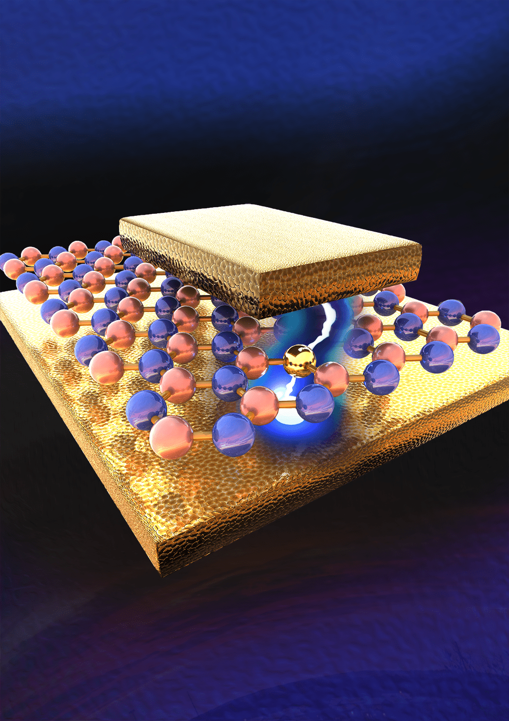
The researchers took several measures to ensure the quality of their sample devices. They grew h-BN monolayers directly on the bottom electrode and then grew the top electrode directly on the h-BN to avoid any impurities and defects arising from transfer processes. They also used gold, an inert metal, for their electrodes. This helped to rule out the role of oxides forming at the interface so the researchers could attribute any switching behaviour to the h-BN layer with certainty.
“After many rounds of sample experiments we were able to work on high-quality h-BN monolayer films grown by collaborators at University of Texas and also samples from Peking University that resulted in observation of memory effects in the thinnest atomic monolayer, a materials science record,” says Akinwande.
Resistive switches gain functionality on paper

Filling in the gaps
Measurements of the effect of temperature on the electronic properties revealed that while the devices shared the characteristics of TMD devices in the low resistance state, in the high resistance state the behaviour differed. The increasing current with temperature in the high-resistance state suggests the role of charge traps in the electronic behaviour.
Based on ab initio simulations the researchers explain the switching behaviour as the result of boron vacancies. In the low resistance state, gold atoms can occupy these vacancies forming a conductive bridge.
The ratio of the high and low resistance states was 107. Switching occurred in less than 15 ns, and tests demonstrate that the resistance states were stable for at least a week after over 50 switching cycles. “We are now conducting further experiments to improve the reliability and explore applications including and beyond information storage,” says Akinwande.
Full details are reported in Advanced Materials.