This year the Materials Research Society will replace its traditional Boston-based Fall Meeting with a virtual conference and exhibition

For nearly 50 years, researchers from around the world have converged in Boston for the Fall Meeting of the Materials Research Society. This year, however, as a result of the Covid-19 pandemic, the meeting will be convened as a fully digital event in combination with the Spring Meeting, which was due to take place in Pheonix, Arizona, back in April.
The joint 2020 MRS Spring/Fall Meeting & Exhibit, scheduled for 27 November ̶ 4 December, will include the scientific programmes from both meetings, with a combination of live and on-demand presentations. John Rogers of Northwestern University will give a plenary lecture on functional materials that enable small electronic devices to be integrated into the body, while a range of networking, Q&A sessions and professional development events are available to access before and after the meeting.
A virtual exhibit will enable attendees to interact directly with equipment vendors, with extended “booth hours” where delegates can chat with company representatives. It is also an ideal opportunity to up to date with the latest technology developments – a few of which are highlighted below.
Turnkey system delivers fast and precise Hall measurements
A fully integrated measurement platform from Lake Shore Cryotronics makes it quicker and more convenient to acquire high-precision Hall measurements. Ideal for anyone studying semiconductor materials, the MeasureReady FastHall Station incorporates Lake Shore’s M91 FastHall controller into a tabletop system that enables simplified Hall measurements and reduces the time needed for experimental setup.
Along with the M91 measurement controller, the all-in-one station includes a Windows-based computer, a 1 T permanent magnet, a high-precision sample holder, and all the necessary software and cabling to provide a comprehensive range of Hall measurements. The system can detect sample resistances up to 1 GΩ and mobilities as low as 0.01 cm2/V s –making it ideal for research into low-mobility materials.

Lake Shore’s patented FastHall method speeds up measurement times, while easy-to-use spring pin and solder sample holder cards accommodate up to 10 mm × 10 mm van der Pauw and Hall bar type samples. The station also features an electronically shielded, low-noise sample space with guarded contacts, making it quicker and easier to derive accurate measurements of the carrier type, carrier concentration, mobility, and Hall coefficient.
The system’s MeasureLINK-MCS software collects all the data, and provides standard sequences, charts, and test scripts that can be customized by the user. In addition to performing complete Hall analyses and outputting all measured and derived values, detailed reports can be generated that include all the supporting intermediate data, so a researcher can readily confirm the integrity of the results. Optional extras include a gate-bias instrument plus a liquid-nitrogen add-on to convert the standard room-temperature station to a cryogenically cooled sample space maintained at 77 K.
Large-sample AFM pinpoints polymer properties
Atomic force microscopy (AFM) has become a crucial tool in both research and industry for studying the properties and structure of many different materials and devices. In an online presentation that is now available to view on demand, Dr Vladimir Korolkov, a senior application scientist at AFM manufacturer Park Systems, highlights the use of AFMs to study the structure of polymer materials.
In the presentation, Korolkov explains how to exploit an AFM to resolve individual polymer chains in real space, which is particularly important because the properties of polymer materials are strongly influenced by the packing and conformation of individual macromolecules as well as their monomer composition. He also shows how an AFM can be used to acquire ultrahigh-resolution images of individual PTFE molecules on the semi-crystalline surface of a commercial Teflon tape.
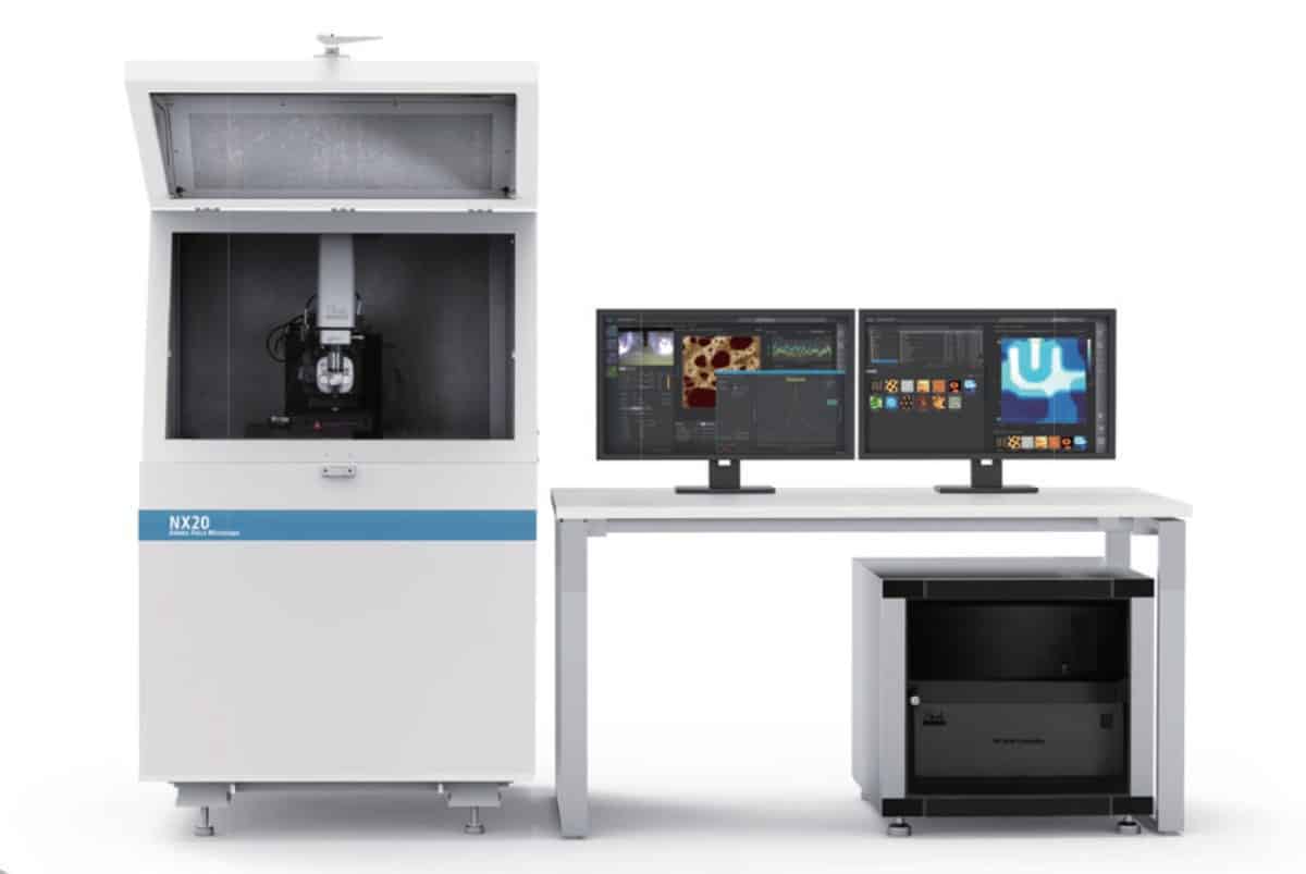
Using these real-world polymer samples, Korolkov highlights the capabilities of Park Systems’ NX20 AFM for high-speed acquisition of high-resolution images. The NX20 is designed to study large samples and conduct multi-sample analyses, and comes with an automated interface that makes it easy for non-experts to acquire high-quality data. The instrument supports single-click imaging through the auto mode of Park’s SmartScan software, while automatic operation of the cantilever brings it safely into contact with the surface within just 10 seconds.
The NX20 also controls the scan speed based on the peaks and valleys of the sample surface, minimizing the scanning time while also acquiring a high-quality image. When moving to a neighbouring location or zooming into a target, the system automatically applies a new optimal condition.
Single instrument combines AFM with scanning microscopy
A unique atomic force microscope (AFM) from Quantum Design can easily be integrated into the high-vacuum environment of almost any scanning electron or scanning ion microscope (SEM/FIB). The AFSEM® Nano enables simultaneous operation of SEM, FIB, and AFM inside the vacuum chamber, allowing these complementary techniques to be combined without needing to transfer the sample or break the vacuum.
The AFSEM Nano directly correlates AFM functionality to SEM or FIB information at the same location on the sample. This correlated functionality allows users to, for example, measure the real 3D-topography of their sample with (sub)-nanometer resolution inside their SEM or FIB system, or easily identify the region of interest with the SEM and then use the AFM to measure the physical, electrical, or magnetic properties at the same location.

Combining the different techniques makes it easy to analyse samples with very different shapes or sizes. Users can also obtain in-situ correlation of chemical (EDX) and crystallographic (EBSD) information, and achieve 3D subtractive tomography by combining FIB slicing with the mapping of nanomechanical properties using the AFM.
The AFSEM Nano is a laser-free AFM that exploits a self-sensing cantilever technology to avoid the need for optical alignment inside the vacuum chamber. Its open design allows for easy integration with other optional add-ons, such as tensile stages, nano-indentors or nano-manipulators.
Materials matter for 2D layered perovskite research
2D layered perovskites have attracted huge research interest for their unique optoelectronic properties, helped enormously by the discovery that the most promising structures – usually hybrid organic–inorganic lead halides – can be prepared easily and cheaply using solution processing techniques. Photoluminescent 2D perovskites have a direct bandgap with a narrow emission peak that can be tuned by changing the layer thickness and the material composition, and have been widely studied for applications in light-emitting diodes, phototransistors, lasers, and solar cells.

Materials company MilliporeSigma offers a range of fully synthesized layered 2D perovskites, including some of the most popular organolead halides. Also available is a comprehensive portfolio of precursor materials, including lead halides, organohalides, and halide acids, as well as other key materials needed to fabricate 2D layered perovskites.