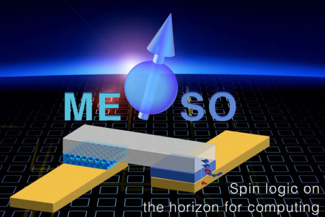
Researchers at Intel Corp. and the University of California at Berkeley have invented a new kind of computing device based on magnetoelectric spin-orbit logic (MESO). The device, which works at room temperature, is made from multiferroic and topological materials and it could be 10 to 100 times more energy efficient than future microprocessors that are based on conventional CMOS (complementary metal-oxide-semiconductors). It is also able to host five times more logic operations than a CMOS chip of the same size.
Transistor technology was invented 70 years ago and is ubiquitous in our modern world. Since the early 1980s, most electronic devices have relied on CMOS-based transistors – in which the resistance of a semiconductor is modulated by applying a voltage across an insulating gate. This switching technology continues to be the mainstay in electronics even though transistors have become ever smaller over the decades and can now be just 10 nm in size.
This successful size scaling has come with a price, however, and voltage and frequency scaling has slowed. Further decreases in operating voltages are not possible because of the so-called Boltzmann limit of current control (which is 60 mV for every change in current by a factor of 10 at room temperature). Researchers are thus looking for alternative technologies.
Collective switching devices
“Finding the next room-temperature general purpose switch that allows for computational scaling is a holy grail for computing,” says team member Sasikanth Manipatruni, who is responsible for hardware development for the MESO project at Intel in Hillsboro, Oregon, and who designed the first ever MESO device. “So-called collective state switching devices are potential candidates for replacing or enhancing CMOS-based transistors. A collective state switch is one that operates by reversing a material’s ferromagnetism, ferroelectricity or ferrotorodicity, for example. Such devices could be made smaller than 10 nm and overcome the ‘Boltzmann tyranny’.”
Multiferroics show promise in this context since they contain atoms that have more than one collective state. Positive and negative charges are offset in these materials and create electric dipoles that align throughout the sample, so producing a permanent electric moment.
The MESO device made by Manipatruni and colleagues comprises a multiferroic consisting of bismuth, iron and oxygen (BiFeO3) that is both anti-ferromagnetic and ferroelectric. “These two states – anti-ferromagnetic and ferroelectric – are linked so that changing one affects the other,” explains Ramamoorthy Ramesh of UC Berkeley, who made the first multiferroic material back in 2001. “By manipulating the electric field, you can change the magnetic states, which is critical to MESO.”
Spin-orbit coupling for readout
In MESO devices, the electric field flips the electrical field throughout the material, which in turn flips the electron spins that generate the magnetic field. This capability comes from spin-orbit coupling, a quantum effect that produces a current dependent on the direction of the electron spin.
The researchers are able to read out this direction, and thus the state of their multiferroic, using topological or high-spin–orbit-coupling (SOC) materials with a spin-orbit effect. Such materials include topological oxides.
“We do this by injecting a supply current into the device, which causes spin-polarized electrons to flow from the ferromagnet into the SOC material,” explains Manipatruni. “Thanks to SOC spin-to-charge transduction, a charge current is generated at the output. The input charge state (positive voltage and current) is thus inverted by the MESO logic gate at the output.”
“Many good properties”
Our MESO has many good properties, he says. “First, it is the first scalable spintronic logic device than can meet the demands of integrated circuits for computing, in the sense that the operating principles allow the energy requirement to improve as the device becomes smaller. Indeed, the device’s energy reduces by eight times for every two-fold reduction in size.”
And that is not all: the device can operate at 100 mV, and potentially even lower voltages, he adds. “This switching voltage is five times lower than CMOS with a concurrent energy reduction of 10 to 30-fold. Finally, logic density is also much higher since the device is essentially a single multiferroic and ferromagnet node. In fact, the logic density increases by five times compared to that possible in future CMOS-based devices.”
This class of logic produces a leap in computational efficiency beyond the limits imposed by the physics of CMOS, he tells Physics World. “Our calculations show that it is capable of more than 200 TIOPS/W (trillion integer operations/watt), which means that there could be a 10-100 times efficiency boost across computer platforms. This increase could come in very useful for emerging applications such as self-driving vehicles and drones, machine learning, artificial intelligence and the Internet of Things.”
“We are looking for revolutionary and evolutionary approaches to computing,” adds Intel senior fellow Ian Young, “and are excited to see the path to 100 mV operation for our logic.”
The researchers, who report their work in two papers, one published this week in Nature 10.1038/s41586-018-0770-2, and one last month in Science Advances 10.1126/sciadv.aat4229, say they will now be focusing on improving their technology. “We will continue to work with our internal and external partners at UC Berkeley (Ramesh Ramamoorthy) and Cornell (Darrel Schlom), as well as Felix Casanova’s team at Nanogune, Manuel Bibes and Albert Fert at CNRS/Thales, and other academics that we are trying to involve further. Our hope is to trigger a wave of innovation across industry and academia targeting beyond-CMOS with room temperature quantum materials,” says Manipatruni.


