Invented 20 years ago, nanoimprint lithography offers a powerful manufacturing alternative for the semiconductor and other nanotechnology sectors, says Helmut Schift

It is 50 years since Intel co-founder Gordon Moore observed that the density of transistors in silicon chips doubles every 18 months. This miniaturization trend is driven by the ingenuity of the semiconductor industry to pattern ever-smaller features on silicon wafers, with the latest processors containing several billion transistors with features smaller than 20 nm across. Moore’s “law” became cast into the International Technology Roadmap for Semiconductors (ITRS), which describes the envisaged date of introduction of the benchmark transistor dimensions or “nodes” that define next-generation semiconductor fabrication plants.
The workhorse of the modern chip manufacturing industry is photolithography. Here, light shining through a transmission mask is demagnified and used to project the image of the mask’s absorption pattern on a silicon wafer covered with a photosensitive polymer called a resist. The current ITRS node is 14 nm, which is achieved using light with a wavelength of 193 nm and sophisticated optical techniques to circumvent diffraction limits. Electron-beam lithography, in which focused electrons are used to pattern a resist directly, offers a higher resolution than photolithography, but the difficulty in producing large volumes of wafers typically limits the technique to mask-generation or research purposes.
Alternative needed
For some applications, however, lithography is too costly and does not provide sufficient resolution and/or throughput. This is particularly true in the case of large-area applications such as magnetic media, as in the surfaces of hard disks, where patterning has not been used until now and additional costs need to be kept within a few cents per device.
Nanoimprint lithography (NIL) is a high-resolution parallel patterning method that offers an alternative manufacturing technique. Unlike electron- or photon-based lithography, it works by replicating the surface topography of a stamp into a viscous material by direct mechanical contact and 3D material displacement. Yet NIL is still similar enough to standard lithography to permit the use of the same manufacturing and technology base: it uses a thin polymer resist for pattern transfer into the underlying substrate by etching or for metal interconnects by electroplating, for instance.
NIL was invented and demonstrated in the 1970s by Susumu Fujimori at NTT in Japan, but it was not until 1995 when Stephen Chou and co-workers then at the University of Minnesota (now Princeton University) published their first results that NIL started to gain broader attention. By demonstrating 10 nm-imprint capabilities at a time when 50 nm was considered the resolution limit of photolithography, NIL was considered as revolutionary – and still is.
In 2003 NIL was named as one of the “10 emerging technologies that will change the world” by the MIT Technology Review, and the technique was added to the ITRS roadmap for the 32 nm and 22 nm nodes. When the industry switched to the 22 nm node, it chose to stick with photolithography. But NIL remains on the ITRS roadmap for smaller nodes and many believe that NIL can replace traditional high-end lithography in semiconductor manufacturing. Indeed, extreme ultraviolet lithography is still struggling to meet the goals of the 14 nm ITRS node because of technological problems with masks and the light source.
For NIL to ever replace such an established technology paradigm as photon lithography, though, it has to obey Moore’s law by allowing further downscaling in resolution. It also has to match the performance – in terms of throughput, precision of overlay, defectivity and reliability – of existing lithography and other techniques.
The high resolution demonstrated by NIL seems to be limited only by the availability of suitable stamps, however, and since NIL does not suffer from diffraction effects, it avoids distortion and failure caused by features in the stamp being too close together. As a contact-based method, it faces serious challenges in controlling the displacement of the viscous material by squeeze-flow or capillary forces during moulding and also during the detachment of the stamp after the resist material is solidified. The major obstacle for the introduction of NIL, however, seems to be defectivity: small particles either in the environment or in the resist must be filtered out to meet the required tolerances for high-yield semiconductor manufacturing.
During the past 10 years the venture capital company Molecular Imprints, based in Austin, Texas, has invested huge resources in this area. In 2014 the firm was bought by lithography-tool provider Canon, which will help NIL to meet chip-maker requirements for next-generation devices. Recently, Toshiba has expressed a commitment to use NIL for the manufacture of NAND flash memory in 2016, followed by DRAM memory and logic.
Large-area applications
From the beginning it has been clear that semiconductor manufacturing is not the only target for NIL. Indeed, after 20 years of development, NIL tools are already installed in almost every clean-room research facility. Typically, they are used for the small-scale fabrication of nano-optical devices with diffraction gratings, photonic crystals and plasmonic sensing areas. Surface patterning of polymeric substrates with anti-wetting properties or bio-chips with nanofluidic channels for use in blood or DNA analysis are other NIL applications that are either too costly or not possible using standard lithography.
Since NIL was invented, European companies such as Obducat, EV Group, SUSS MicroTec and Jenoptik have developed NIL tools for research and small-scale production purposes, sometimes simply by converting existing tools for photolithography. These tools allow entire wafer-sized stamps and substrates to be imprinted, and several firms are now providing automated NIL tools for 150–300 mm wafer-like stamps and substrates for applications quite distinct from semiconductor manufacturing. In addition, several companies including NILT, Eulitha, Temicon, AMO and Micro Resist Technology are providing the materials and stamps for this growing NIL market.
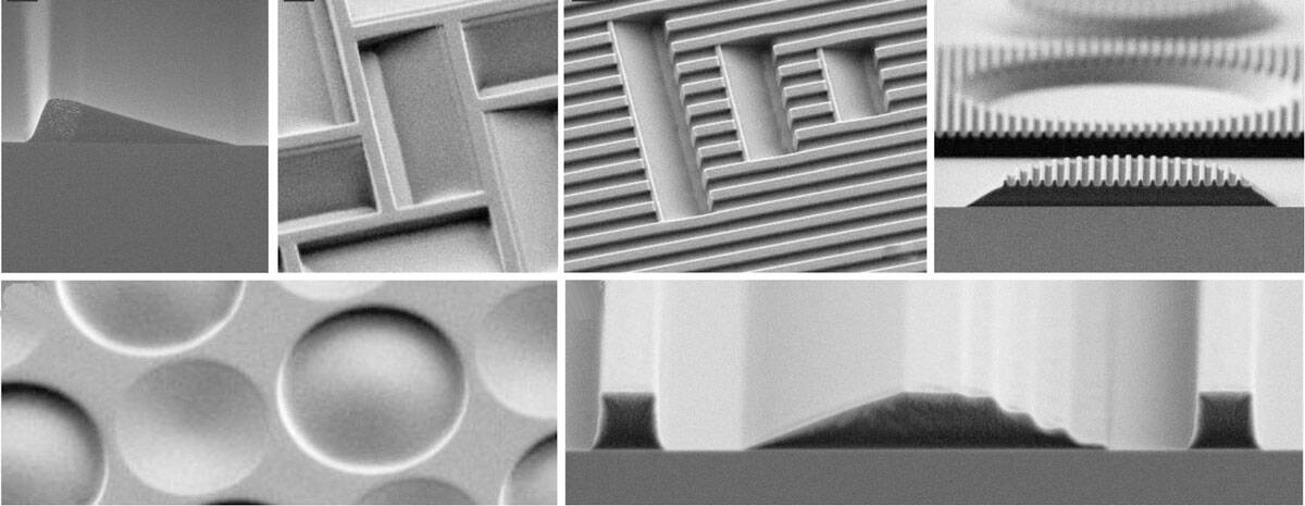
Whereas NIL-based semiconductor chip patterning requires a small stamp that is repeatedly imprinted until the entire wafer is fully covered (a so-called step-and-repeat process that demands successive chip levels to be aligned within a few nanometres), new applications such as large-area wire-grid polarizers for displays, high-brightness light-emitting diodes (LEDs), or patterned magnetic media only need single-layer patterning with a stamp that covers the full size of the substrate. For hard-disk applications, for instance, the full surface area of the disk has to be covered with 15 nm-wide magnetic data bits arranged in concentric circles – a process that would take several weeks using electron-beam lithography.
Cutting costs
For LED production, which is much simpler than patterned magnetic media, NIL has already been successful in replacing photolithography because it offered lower costs when the industry switched from 100 mm to 150 mm wafer formats. The sapphire substrates are currently patterned to enable defect-free epitaxial growth of the active gallium-nitride LED layers, but in the future it is likely that photonic-crystal patterns will be employed on the top of the LEDs to enhance light extraction. Resolutions of several hundred nanometres have been demonstrated, but this is expected to decrease as the technique is taken up by other industries. Recently, for instance, the German firm ULM Photonics (which is part of Philips) established NIL as its production method for polarizing gratings on vertically emitting semiconductor lasers.
NIL has thus proved successful in completely different applications from semiconductor manufacturing, where extreme resolution and the overlay of different levels do not play such a big role. Thanks to the range of optical effects possible with diffractive gratings or specific surface textures, numerous further applications seem possible. These include antireflective coatings on screens, solar cells with improved efficiency, “Gecko” surfaces with engineered adhesion, “shark-skin” surfaces that reduce drag in water, and even LEGO bricks with structural rather than pigment-based colouring.
NIL for the future
These applications, along with many bio-applications such as surface patterns for controlling cell growth, seem a world away from the original NIL process. They profit from a toolbox for stamp manufacturing that has been established over the past 20 years, which includes 3D surface patterning and replication by different moulding processes such as injection moulding and roll embossing. This has been complemented by European projects such as NaPa and NaPANIL, which have resulted in a “library of processes” that makes NIL more accessible to researchers and engineers.
Killer applications, such as semiconductor chip manufacturing with highly standardized processes and tools, ensure that NIL will continue to drive key industrial domains. Meanwhile, new applications such as hard disks and LEDs will profit from the broad process methods available, which can be adapted to large areas, non-flat surfaces and functional materials.
After 20 years of development, NIL is now mature and is already used on an industrial scale for LED manufacturing. Future progress will depend on it helping with applications that need simple solutions for large areas to be imprinted quickly, and to do so reliably and with few defects. The next five years will prove not only whether NIL has established itself as a technology driver, but also if it has succeeded in changing our thinking about how technologies are integrated into existing and new process chains.