LEDs based on nanowire structures could enable flexible devices, and displays covering a wider range of colours, as well as easing lattice mismatch strains when integrating with silicon. Despite the progress made from investigations of these devices over the past 15 years, further theoretical and computational studies are needed to understand how they can be optimized. Researchers in Finland and Sweden have now demonstrated that certain common assumptions when modelling planar LEDs are not valid for their nanowire counterparts and that sophisticated models are needed that integrate both electronic and wave optic effects.
Effective models are a delicate balance of what can and can’t be safely assumed. When characterizing LEDs people had always assumed an internal quantum efficiency of 100% at low temperatures, and a light extraction efficiency that does not change as a function of temperature. However as Pyry Kivisaari started to discuss nanowire LEDs with Nicklas Anttu during a post doc at Lund University in Sweden, they began to question the validity of these assumptions.
By integrating a model for wave optics with carrier dynamics, Kivisaari, Anttu and co-author Yang Chen at Lund University found that despite the prevalence of assumptions to the contrary, temperature did affect the light extraction efficiency and emission enhancement of their LED devices. “I believe the assumption is justified in LEDs that have a planar active region where there are not such strong wave optical effects in the extraction efficiency,” says Kivisaari. “So this is really nanowire- or nanostructure-specific finding.”
The results were also able to identify significant effects from surface recombination at recombination velocities – a measure of the recombination probability – of 104 cms-1. Kivisaari highlights previous experimental work from researchers at Paul-Drude Institut in Berlin and the Russian Academy of Science who had reported high rates of recombination at temperatures as low as 10 K, resulting in low photoluminescence efficiencies. “We confirm that based on theory this might happen if you have a large enough surface recombination velocity, so you can get low efficiency even at really low temperatures.”
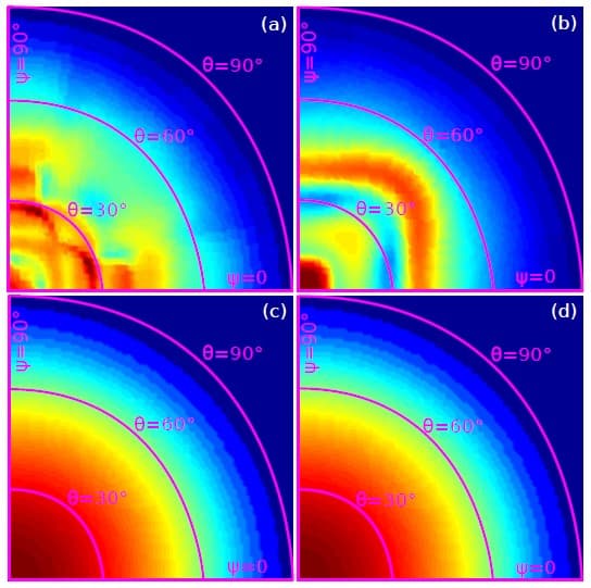
In addition, they found that the angular distribution of the emitted light changed depending on the temperature and the diameter of the nanowires in the array, suggesting for the first time that temperature-controlled angle-resolved measurements could provide important insights for studies of the optical response of these structures.
Combining models
Kivisaari describes Anttu as an expert in the scattering matrix method, a numerical approach for solving the Maxwell equations to calculate how an electromagnetic field propagates in a system. Fortunately Kivisaari’s own expertise lies in carrier dynamics, so they were able to integrate the calculations for the wave optical response of the system with the drift-diffusion equations of electrons and holes in the structure.
At the heart of their approach is the Lorentz reciprocity theory – that the position of a light source and the resulting electromagnetic field can be interchanged without affecting the relationship between them. “We use the reciprocity principle to define how much the emission of light is enhanced in a specific mode,” says Kivisaaari. “The larger the electromagnetic field of the mode in the nanowire structure, the stronger the emission, so we calculate an enhancement factor based on the electric field, which we then plug in into the electron-hole recombination model or formulae.”
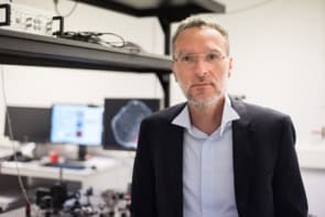
Using the reciprocity principle in this way, the model closely resembles what might be calculated for a solar cell, and Kivisaari believes there is likely much that can be learned about LEDs from solar cell research and vice versa. “The authors present an impressive computational method to analyse and design optoelectronic nanowire devices,” says Bernd Witzigmann – a world expert in nanowire research who heads the Computational Electronics and Photonics Group at the University of Kassel in Germany, and was not involved with the current research. He adds, “Their results highlight the importance of a multi-physics method that includes electromagnetic, electronic and thermal phenomena. Even more, in nano-devices, some of these phenomena are closely coupled, as shown in the emission features of a nanowire array LED. Computational design is a pre-requisite in order to exploit the full potential of an exciting technology.”
Next steps
Kivisaari is keen to come up with new device structures, especially based on diffusion-driven charge transport, and develop better simulation models. He is now a member of a group at Aalto University focused on electroluminescent cooling, where light carries away heat. He hopes to develop his model to understand the optoelectronics in those structures too, as well as emerging materials such as molybdenum disulphide. He remains motivated by technology that benefits the environment, such as photocatalytic water splitting to produce hydrogen fuel, which can also exploit nanowires and is another area he finds interesting for future work.
Full details of the combination model are available in Nano Futures.

