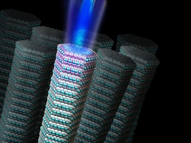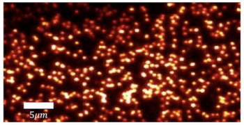
Researchers at Lund University, Sweden, have grown single continuous GaAs nanowires consisting of segments of pure wurtzite and zincblende phases. Using photoluminescence spectroscopy, they found that the spatial confinement along the radius of a nanowire resulted in bending of the band structure of the material.
Wurtzite/zincblende GaAs interface
Since it is only in recent years that phase-pure wurtzite and zincblende GaAs have been grown successfully, we have yet to uncover many fundamental properties of these materials. However already the staggered alignment of the conduction and valence bands at the interface between wurtzite and zincblende GaAs – type II heterojunction characteristics – is attracting interest for potential use in future electronic and optoelectronic devices.
When the wurtzite phase is sandwiched between the zincblende phase, the minimum of the conduction band and the maximum of the valence band are physically separated in the two different materials. Such an alignment of the energy bands aids the separation of photo-induced electron−hole pairs across the interface of the heterojunction, which is necessary for photovoltaic applications.
Photoluminescence spectroscopy of the nanowires
To investigate nanowire size effects on the band separation, lead author Irene Geijselaers and her team performed photoluminescence spectroscopy on a number of GaAs nanowires with diameters ranging from 70 nm to 150 nm.
They grew the nanowires by metal-organic vapour phase epitaxy (MOVPE) using gold nanoparticles as the catalyst. By simply varying the concentration of the As-precursor in the MOVPE growth reactor, the researchers could switch between growing either the wurtzite or zincblende GaAs phases. This method does not require any changes in growth temperature (which can result in strain and subsequently defects in the nanowire) and creates atomically sharp interfaces between the two phases. In addition, they could control the diameter of the nanowires with the diameter of the gold catalyst nanoparticles.
As the diameter of the nanowire increased, they found the transition energy (the measured energy gap between the conduction and valence bands) decreased. The researchers explained the result as being due to an increase in bending of the band structure in thicker nanowires compared with thinner ones.
In the paper, the authors remarked, “our results will improve accuracy of future modelling of electronic properties of wurtzite-zincblende GaAs heterostructures and other engineered polytypic materials.”
The research is detailed in Nano Futures 10.1088/2399-1984/aac96c.


