Jin-Woo Han is senior scientist at NASA’s Ames Research Center in California’s Silicon Valley. Along with colleagues Meyya Meyyappan, Myeong-Lok Seol and Jungsik Kim, he has designed a nanoscale complementary vacuum field emission transistor (VFET). In this interview Han explains why his team is interested in VFETs and the challenges involved in creating the devices

What is a VFET?
A vacuum field emission transistor (VFET), also known as nanoscale vacuum channel transistor, is a device with no semiconductor channel. Instead, it has an empty gap between the source and drain terminals. Electrons tunnel through this empty space.
Vacuum diodes and triodes have long been known and used in numerous applications. Recently, researchers have combined the best of vacuum physics and modern integrated circuit manufacturing to produce VFETs on wafer scale with extremely small dimensions (for example, source-drain distance of less than 50 nm). This is smaller than the mean free path in air at atmospheric pressure. Thus, these small devices work under atmospheric pressure without the need for vacuum; nevertheless, for stable and reliable operation over time, moderate vacuum levels such as few hundred millitorr may be desirable. These VFETs work on small drive voltages such as 2 V, which is unheard of in vacuum electronics.
A wide variety of materials including silicon, silicon carbide, gallium nitride, graphene and carbon nanotubes have been considered as emission sources in constructing devices with either horizontal or vertical configurations.
What is a complementary device and why has it not been possible to create a complementary VFET?
In conventional metal oxide semiconductor field effect transistors (MOSFETs), we have n-type and p-type devices –NMOS and PMOS respectively. This is readily possible since semiconductors can be doped either way. The availability of these two types allows construction of a CMOS with the two devices working as a pair. When connected to a common input voltage, they work in opposite fashion: when one transistor is on, the other is off. This allows the CMOS to operate using less power.
Complementary operation of VFET has not been possible because there is no semiconductor material in the channel for doping and no possibility to create holes to make a p-type device. VFET is unipolar since it is electron only.
How does your design overcome these challenges?
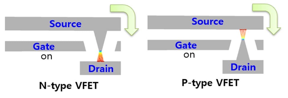
The primary (or the only) source of carriers in a vacuum device is electrons, resulting from the field emission in the source electrode. In the absence of holes, we need an external mechanism to invoke complementary operation (see figure below). That mechanism here is the nanoelectromechanical (NEM) actuation of the gate that modulates the vacuum channel length and resultantly the electron transport across the source-drain channel with the gate voltage. A shorter vacuum channel length is formed, and a positive input voltage turns on the n-type device and a negative input voltage turns on the p-type device.
The NEM-driven gate modulation is a successful technology employed in NEMS-relay switches and other low power electronics.
Are you currently fabricating devices based on this design, do you have any preliminary results?
Not yet. We have so far demonstrated the concept using simulations and studying potential circuits. This works well as in CMOS, providing complementary type transfer and output characteristics. Device fabrication is next. We have provided a possible process flow to fabricate the devices, and the process steps are very similar to those currently in use in silicon integrated-circuit manufacturing. We expect that the device research community would come up with their own tweaks to both the design and process flow and their choice of material systems.
What are some possible practical applications for the device, if it can be successfully fabricated?
First, compared to electron-only conventional operation of VFET, this complementary operation will enable low static power consumption and high noise immunity, both of which are important in applications using logic circuits. Thus, low-power logic circuit application is one possibility. Also, the VFET is ideal for radiation-immune electronics needed in space and military applications.
Vacuum technology comeback immunizes nanoelectronics from radiation

Why are VFETs immune to the effects of radiation?
Radiation strike on conventional solid-state devices creates all sorts of defects on the channel semiconductor and oxide materials. Depending on the type of defects and damage created, the effect can slowly accumulate and lead to malfunctions or can result in a catastrophic device failure. Absence of a semiconductor channel or dielectric material in the VFET makes it immune to radiation.
The design is described in ACS Applied Nano Materials.