A new technique to extract information on the mobility of electrons and holes in semiconductors has unlocked a long-held secret in the Hall effect 140 years after it was discovered. The carrier-resolved photo Hall (CRPH) measurement, as it has been dubbed, involves shining light with a known illumination intensity on a sample. The work could help in the development of next-generation semiconductor technology, such as improved solar cells and optoelectronics devices as well as new materials and devices for artificial intelligence (AI) hardware.
“Our discovery can be expressed in a succinct equation, Δμ = d(σ2H)/dσ, which gives us information on the difference in the mobility of holes and electrons in the Hall effect in semiconductors when illuminated with light,” explains study lead author Oki Gunawan of the IBM T. J. Watson Research Center in Yorktown Heights in New York. “The finding is critical because this ‘photo-Hall two-carrier transport’ has been a long-standing unsolved problem in solid-state physics until now.”
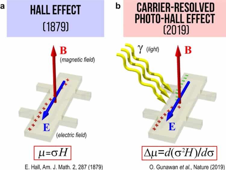
The classic Hall effect occurs when an electric current flows through a conductor in a magnetic field. If the current and magnetic field are at right angles to each other, the Lorentz force deflects the electrical charges (electrons or holes) to one side and a Hall voltage builds up in the direction that is at right angles to both the current and the magnetic field. This voltage is named after Edwin Hall, who discovered it back in 1879.
In the classical Hall measurement, researchers measure the longitudinal and transverse resistance of material (typically in the form of a Hall bar) to obtain the conductivity, σ, of the sample and its Hall coefficient, H, respectively. This measurement provides fundamental information on: the majority charge carriers in the material (electrons or holes depending on whether the material is n- or p-type); the speed under an applied electric field, or mobility, μ, of these charge carriers; and their density (n). Unfortunately, the standard Hall measurement only provides information on majority charge carriers.
New technique provides more information
Gunawan and colleagues’ new technique provides information on the mobility of both types of charge carrier, as well as photocarrier density, carrier recombination lifetime (the process by which electrons and holes annihilate with traps or each other) and the diffusion length for electrons, holes and ambipolar carrier types.
“In our work, we repeat the measurements of conductivity and Hall coefficient as a function of the intensity of light we shine on the sample,” explains Gunawan. “When light is shone on a semiconductor, both electron and hole pairs are generated and the σ-H curve we obtain provides new information on the mobility difference between the holes and electrons, Δμ, thanks to the Δμ = d(σ2H)/dσ equation.
Gunawan says he discovered the equation thanks to a gedanken or thought experiment in which he imagined two otherwise identical p-type materials with one of the materials having a minority charge carrier mobility that is twice as fast as the other.
σ-H curve contains minority carrier information
“In the dark, both materials have the same σ-H point and you can’t tell the difference between them, since of course, there are no minority carriers in the dark,” explains Gunawan. “With increasing light intensity, however, the σ-H curves of both materials diverge and the trajectory of the σ-H curve (and its slope) then contains minority carrier information, according to Δμ = d(σ2H)/dσ.”
With this discovery we have a new technology to extract even more precious information from semiconductors, he tells Physics World. “We can now use the three most common excitation sources in physics: electric- and magnetic fields – which were already used before – and now light to provide us with a more complete understanding of these materials.
“Just as the classical Hall effect is widely employed in physics and semiconductor labs around the world, so our technique could also be widely applied to help advance R&D efforts on electronic materials,” he adds.
“The technique might even be a new chapter in electronics materials research. Before now, we had to make use of various separate tools – such as time-resolved photoluminescence and terahertz spectroscopy – to obtain some of the seven parameters mentioned above. And we could only obtain partial information, with the results often being complicated to analyse because these techniques do not use steady-state light illumination.
“With our new CRPH technique, we can obtain all seven parameters as a function of light intensity in a single experimental sitting and on a single sample.”
Rotating parallel dipole line Hall system
The core technology in this work is based on recently developed rotating parallel dipole line (PDL) magnets that serve as a highly sensitive AC field Hall system. “This system is very critical for high-sensitivity photo-Hall measurements on low mobility polycrystalline materials, for example,” explains Gunawan. “The system also has an emerging application (and is the subject of ongoing research at IBM) for developing AI hardware devices in which the key materials are no longer silicon.”
Exploring innovation, from taxis to data centres

The team, which also includes researchers from KAIST (Korea Advanced Institute of Science and Technology), KRICT (Korea Research Institute of Chemical Technology) and Duke University, says it now wants to apply its technique to a broader variety of materials, including emerging photovoltaics and materials for AI hardware devices.
“We also want to find out more, for example, on what happens if the mobility of the charge carriers in a material is not constant, as we initially assume. There could also be many more non-ideal cases that we could investigate.
“Another equally important topic is to understand the limitations of CRPH. Indeed, it may not work in metallic materials, which require extremely strong laser illumination that could melt them. There could also be other limitations that we need to identify.”
Full details of the research are reported in Nature 10.1038/s41586-019-1632-2.