A new, low-cost and industry-compatible process to make flexible and semi-transparent silicon-based circuits has been unveiled by researchers at the King Abdullah University of Science and Technology in Saudi Arabia. The technique is an important step forward in making high-performance flexible and transparent computers, says the team.
The last decade has seen considerable progress in flexible electronics, with a host of novel applications such as electronic paper-like displays and artificial skin having already seen the light of day. However, most of these devices are made from organic materials such as polymers, carbon-based nanowires and carbon nanotubes, rather than inorganic silicon – despite the fact that this element is the basis of most modern technology. This is because silicon is intrinsically brittle and rigid, meaning that it does not easily lend itself to flexible applications.
Organics are too slow
The problem with organic flexible-electronics devices, however, is that they are much slower than their silicon counterparts. They are not very robust at higher temperatures either and cannot be formed as continuous films – unlike bulk silicon. Integration densities (the number of transistors that can be packed onto a single chip) for these materials are also much lower than those for the silicon-based transistors found in today’s microprocessors.
Although inorganic flexible electronics do exist, they rely on expensive substrates such as SOI, UTSOI and silicon (111), and the processes to fabricate ultrathin silicon or porous silicon are far from straightforward.
Now, a team led by Muhammad Hussain could have gone a long way in overcoming these fundamental problems with a new method that employs traditional state-of-the-art CMOS-compatible processes that transform silicon-based circuits into flexible and semi-transparent ones while still retaining silicon’s excellent electronic properties. Costs are also kept low because the technique makes use of the most common substrate employed in the semiconductor industry today: bulk monocrystalline silicon (100) wafers.
Deep trenches
Hussain and colleagues made p-type metal–oxide–semiconductor field-effect transistors (MOSFETs) by first gorging deep trenches less than 50 µm wide on a silicon-dioxide layer (the active layer in the circuit). Next, they added a high-dielectric/metal gate stack on top of this layer using atomic-layer deposition. The deposited films are then pattered using reactive-ion etching down to a resolution of 5 µm ready to receive the different device components.
The next step involves implanting dopant ions to form source and drain electrons in the active area and these electrodes are contacted to the substrate using nickel-silicide film. Holes are created in the contact pads and then over the entire sample surface. Deep reactive-ion etching is finally employed to create straight channels about 30 µm deep in the silicon substrate.
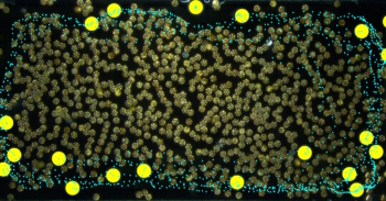
A thin silicon film (containing all the device elements) is then released from the bulk substrate, again using etching. This film is flexible and semi-transparent thanks to the network of etch holes.
Fast and flexible
The researchers tested the electronic and mechanical properties of their devices and found them to have a 80 mV/dec sub-threshold slope – which is the fastest ever switching demonstrated in a flexible transistor. “What is more, the devices have the lowest bending radius compared with any other flexible transistor made to date – including plastic ones,” Hussain told physicsworld.com.
John Rogers of the University of Illinois, who was not involved in this work, comments that the devices “do not only demonstrate mechanical flexibility, but also remarkable levels of optical transparency. The ideas outlined here add to the growing toolkit of approaches and materials for making flexible integrated circuits, with excellent performance.”
The results are an important step forward in realizing a fully flexible computer, adds Hussain. Indeed, the Saudi Arabia team says that it is now working on making integrated systems such as foldable computation and communication devices using its flexible and semi-transparent silicon.
The results are detailed in Nature Scientific Reports.