High-performance lasers are central to both lidar sensing and laser processing – technologies that enable a range of smart mobility and smart manufacturing applications. Lidar, for example, plays an essential role within autonomous vehicles, construction machines and automated factory robots, while laser processing is used for fabrication of electronics, automobiles and solar cells.
Currently, however, the lasers used for these applications – semiconductor lasers, CO2 lasers and fibre lasers – all come with limitations. Speaking at the recent Photonics West LASE conference, Susumu Noda from Kyoto University described the problem.
To generate high-power from a conventional semiconductor laser, such as a broad-area Fabry–Pérot laser, the cavity width must be increased, which results in a low-quality, divergent output beam. “For lidar sensing, a complicated lens systems and fine adjustments are required to reform the beam shape,” Noda explained. “And for laser processing, the output beam cannot be focused sufficiently and thus cannot be used directly for manufacturing.”
Laser processing is also performed using CO2 and fibre lasers. But CO2 lasers are extremely large and have low efficiency. Fibre lasers, meanwhile, contain hundreds of laser diodes that are combined into an amplification fibre. As such, fibre lasers suffer from a complex configuration and a substantial size, as well as limited efficiency.
What’s needed is a totally different laser technology that addresses these issues. And according to Noda, this is the photonic crystal surface-emitting laser, or PCSEL.
PCSELs are new type of semiconductor laser that contain a photonic crystal integrated on top of the active layer. Photonic crystals are nanostructured materials in which a periodic variation of the dielectric constant (formed, for example, by a lattice of holes) creates a photonic band-gap. The resulting PCSELs emit a high-quality, symmetric beam with narrow divergence.
“For lidar applications, lens-free, adjustment-free operation is possible. And for laser processing, due to their high brightness, we can use PCSELS directly for materials processing,” said Noda. “Therefore, photonic crystal lasers are expected to contribute to the development of smart mobility and smart manufacturing.”
Noda and his research team have been working on PCSELs since 1999, when they first established 2D surface-emitting coherent oscillation. They went on to demonstrate control of polarization and beam shape by tailoring the phonic crystal structure, expansion into blue–violet wavelengths and 1D beam steering. In 2013, 0.2 W PCSELs became commercially available, and the team has since demonstrated watt-class operation and above.
Lidar applications
To generate the high-brightness operation required for lidar applications, Noda’s team created a double-lattice PCSEL, containing two sets of square lattice structures with different air hole depths and sizes. The 500 µm-diameter device exhibited a slope efficiency of 0.8 W/A and extremely narrow beam divergence of 0.1°.
The PCSEL demonstrated superior temperature performance to conventional semiconductor lasers, operating between -40 and 100 °C, with temperature dependences of the output power and lasing wavelength of -0.36%/K and 0.08 nm/K. Examining lens-free light propagation from these PCSELs revealed that they could create small beam spots (5 cm) at distances of up to 30 m. Conventional Fabry–Pérot lasers could not even deliver a beam at 10 m or further.
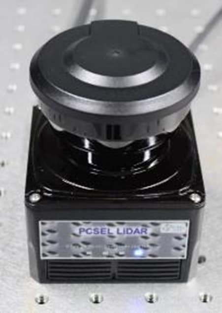
The team used this double-lattice PCSEL to construct a lidar system. Noda pointed out that while conventional lasers used in lidar require complicated lens systems and mechanical mirrors to steer the beam, PCSELs offer lens-free, adjustment-free beam control.
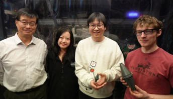
Noda shared a video showing the ability of PCSEL-based lidar to measure the distance of objects – in this case, two researchers. As they walked towards the lidar system, it accurately detected their movement in real time. It could also track smaller changes in distance, such as swinging of arms or hand movements, demonstrating successful high-resolution lidar operation.
The team has also recently demonstrated 2D electronic beam scanning, based on a chip design with dually modulated PCSELs integrated in a 10 × 10 array.
Laser processing
For laser processing applications, the PCSELs need to offer miniaturization and high efficiency, to address the limitations of CO2 and fibre lasers. Using ultracompact PCSELs, “the realization of handheld laser processing systems can be possible,” said Noda.
Three steps are required to achieve this, he explained: creating 1 mm, 10 W PCSELs with high beam quality; enlarging the devices to 3 mm to reach 100 W output power; and developing associated packaging and cooling technologies.
To create 10 W PCSELs, the team optimized the double-lattice structures by adjusting the size and shape of the air holes. The fabricated device successfully achieved 10 W continuous-wave operation, with very narrow beam divergence. Irradiating a metal surface with the focused PCSEL beam formed extremely fine holes. “We believe this is the first successful processing of a metal surface by a single-chip semiconductor laser,” said Noda.
Next, the team fabricated and packaged a 3 mm-diameter PCSEL. Initial tests on this device under pulsed conditions showed that 150 W output was obtained using only six times the threshold current. Noda predicts that by further increasing the device size to 1 cm, kilowatt-class operation could be achieved.
“For the future, key devices for lidar sensing and laser processing can be made using PCSELs,” Noda concluded.