Researchers in Taiwan say they have created a new chlorophyll-coated graphene phototransistor that is much more sensitive to light than devices made of pure graphene. The researchers believe that the device could provide a blueprint for future graphene-based light sensors. However, some experts in the field are sceptical.
Graphene is a sheet of carbon just one atom thick and the material’s remarkable optical and electronic properties could make it useful for devices such as photodetectors and solar cells. Graphene absorbs photons over a wide range of frequencies and its ability to carry electrons at relativistic speeds means that graphene photodetectors can have very quick response times. However, there is one important challenge facing device makers: pure graphene has a low sensitivity to light. Indeed, only 2.7% of the photons hitting graphene create an electron–hole pair that can then be detected.
To get round this problem several groups have produced hybrid devices by coating graphene with another material that absorbs light more efficiently. In 2011 researchers at Manchester and Cambridge universities showed that a covering of plasmonic nanostructures – patterned metal films – could increase the proportion of light absorbed to nearly 50%. A year later at the Institute of Photonic Sciences in Barcelona, scientists achieved even higher sensitivities using quantum dots – with a slight loss in speed.
Cheap and non-toxic
Now, researchers at the Academia Sinica and the National Taiwan University, both in Taipei, have produced a simple yet effective device by covering graphene with chlorophyll. This is a cheap, non-toxic material extracted from plants, where it plays an important role in converting sunlight into chemical energy.
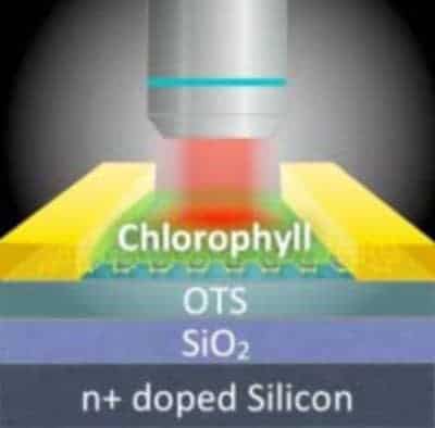
The team’s device is configured as a field-effect transistor (FET). Two gold electrodes attached at either end of a pure graphene flake function as the source and drain. A drop of chlorophyll dissolved in ether is placed on one surface of the graphene. The solvent evaporates to leave a thin film of pure chlorophyll on one side of the graphene. An insulating layer followed by a layer of doped silicon is added to the opposite side to create the gate of the FET (see figure).
By adjusting the voltage applied to the gate, electrons can be drawn from the chlorophyll into the graphene to create n-doped graphene. Changing the voltage to another value causes electrons to move in the opposite direction, making the graphene electron deficient or p-doped. N-doped graphene conducts electricity through the movement of electrons, whereas p-doped graphene conducts through the movement of positive holes.
High gain
When a photon of suitable wavelength hits the chlorophyll, it may create an electron–hole pair. The electron remains in the chlorophyll while the hole is swept into the graphene. If the voltage is set so that the graphene is n-doped, this hole recombines with one of the electrons, thereby reducing the number of charge carriers available and lowering the conductance of the transistor. If the graphene is p-doped, then the hole remains free, thus adding to the number of charge carriers and boosting the conductance.
Graphene has almost no resistance to the flow of charge carriers, therefore adding or removing a small number of carriers has a huge effect on the electric current that can flow between the source and drain. This, says the team, gives the phototransistor a gain of up to 106 when illuminated – making the device extremely sensitive to light.
Commercially viable?
The researchers believe that their results suggest a “feasible method to employ biomaterials for future graphene-based photoelectronics”. Team member Wei-Hua Wang of Academia Sinica accepts it would not be practical to use graphene flakes to make commercial devices because of the laboriousness of the “Scotch-tape method” used to make the flakes. Graphene can also be made using more commercially viable techniques but such materials tend to have lower electron mobility than pure flakes. Although chlorophyll devices made from this graphene would likely have lower gain, Wang says their performance could be comparable to flake-based phototransistors.
Frank Koppens of the Institute of Photonic Sciences questions the advantages of the device over current light-sensitive graphene technologies. “With quantum dots, the devices are quite easy to make at large scale,” he says. “You basically just have to deposit a solution on top of the graphene and then you have a photodetector that has extremely high performance.” He also believes that the limited wavelengths absorbed by chlorophyll could limit practical applications. Alexander Grigorenko, a member of the Cambridge/Manchester team, agrees that the researchers have yet to demonstrate the relative merits of their design.
A preprint of the research is available on arXiv.


