Plasmonic nanoparticle arrays have the potential to improve the emission efficiency of solid-state lighting. Silver and gold nanoparticles were already known to enhance efficiency at visible wavelengths, but they require a complicated, multi-step fabrication process. Now, researchers at the University of Michigan in the US have included plasmonic gallium (Ga) nanoparticle arrays at buried interfaces within semiconducting layers. The nanoparticles can be easily incorporated into targeted areas in a wide range of semiconductor devices. The resulting structures show improved photoluminescence efficiency for emission wavelengths from near-infrared to ultraviolet.
Surface plasmons reveal their secrets
Writing in Journal of Applied Physics, lead authors Myungkoo Kang and Sunyeol Jeon describe how an array of Ga nanoparticles was produced by rastering a Ga+ focused ion beam across a gallium arsenide (GaAs) substrate. The trick is to tilt the beam to an off-normal angle to the substrate, which prompts Ga nanoparticles to self-assemble in close-packed arrays. The diameter of the Ga nanoparticles was controlled by the angle of incidence of the beam on the GaAs surface. Kang and Jeon then grew a layer of GaAs on top of the substrate and the nanoparticles using molecular-beam epitaxy, embedding the Ga nanoparticles within the GaAs material.
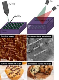
To investigate the effect of nanoparticle diameter and overgrown GaAs layer thickness on photoluminescence efficiency, the researchers used a combination of photoluminescence spectroscopy and electromagnetic computational simulations. They found that the optimal combination of nanoparticle diameter and embedment depth led to improved photoluminescence efficiency compared to high-quality GaAs epilayers without embedded nanoparticle arrays.
Polycrystalline or not?
Structural characterization by transmission electron microscopy revealed that the Ga nanoparticles were amorphous, while the overgrown zincblende-structured GaAs layers were polycrystalline. Usually polycrystallinity is undesirable in such devices, so the team is now working on improving the crystallinity of the overgrown material.
As the researchers point out in their paper, however, “polycrystalline III-V compound semiconductors have been proposed for LEDs in large-area displays. Indeed, this new Ga nanoparticle plasmonics approach would enable polycrystalline gain media deposited on large-area substrates to maintain reasonable light-emitting characteristics. Thus, this approach provides an opportunity to enhance the photoluminescence efficiency from a variety of semiconductor heterostructures.”
The work is detailed in Journal of Applied Physics 10.1063/1.4990946


