Two independent teams of physicists have been able to create and control “plasmons” – collective oscillations of conduction electrons – on the surface of graphene for the first time. Their experimental approach, dubbed “plasmon interferometry”, could be used to study a wide range of materials including superconductors and topological insulators. As the plasmons interact so strongly with light, graphene could be used to create new optical devices and even materials for invisibility cloaks.
Surface plasmons can interact with light at certain wavelengths to create surface plasma polaritons (SPPs), which are light-like excitations that propagate along the surface. SPPs often have shorter wavelengths than the associated light and so tend to confine the light to a smaller region than is allowed in free space. This concentrating effect is particularly useful for shrinking the size of optical circuits and can also be used to create “transformational optics” such as superlenses and invisibility cloaks. Structures that support SPPs have also been used as chemical sensors because they tend to enhance interactions between light and molecules.
Concentrating energy
Graphene – a honeycomb lattice of carbon just one atom thick – is expected to have plasmonic properties that are somewhat different to metals, where plasmons have been studied in detail. This is because the conduction electrons in graphene behave like “Dirac fermions”, which means that they travel through the material at near the speed of light. Graphene plasmons therefore concentrate electromagnetic energy into a much smaller region, which could be useful to researchers developing plasmon-based technologies. Because of these differences, however, conventional techniques for using infrared light to create and study plasmons do not work with graphene.
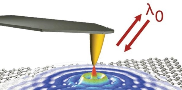
The two teams of physicists have used the sharp tip of an atomic force microscope (AFM) as a nanoantenna, which focuses a beam of infrared light into the graphene. One team includes Zhe Fei, Dmitri Basov and colleagues at the University of California, San Diego, along with collaborators in the US, Singapore and Germany. The other team is led by Frank Koppens of ICFO in Barcelona and includes scientists from CSIC in Madrid and the nanoGUNE research lab in San Sebastian.
Sharp tip
The AFM tip also interacts with plasmons that are already in the graphene and this affects how infrared light is reflected back from the tip to a detector. The teams can therefore detect plasmons in the material by scanning the tip across the surface of graphene and making measurements at a large number of locations. At each location, plasmons created at the tip radiate across the graphene like ripples on a pond until they are reflected at the edges. This creates an interference pattern of standing waves – an image of which is built up by scanning the AFM tip across the samples.
In both experiments the physicists found that the wavelengths of the plasmons are much shorter than those created by shining infrared light on metals – confirming the idea that graphene plasmons concentrate electromagnetic energy into a much smaller region than metal plasmons. The researchers were also able to tune the wavelength and amplitude of the graphene plasmons by changing an applied gate voltage, which could lead to the development of transistor-like devices in which light can be controlled electrically. While the properties of metal plasmons can be controlled by changing the size and shape of metallic nanostructures, such electrical tuning has not been demonstrated in metals.
“The gate voltage changes the density of mobile electrons in graphene,” explains Basov. “With more free electrons in the graphene, its electronic liquid becomes more ‘rigid’ and the wavelength of plasmonic oscillations is reduced, whereas their amplitude is enhanced.” One important consequence of this is that the gate voltage can be used to switch the plasmons on and off. As a result, Koppens believes that the research could lead to ultrafast optical switches. Other applications include better sensors and new quantum-information processing systems.
As for Basov, he is keen to develop plasmon interferometry as a new tool for studying a wide range of materials. “This new approach will be equally useful to probe the surface physics of many other exotic and interesting materials, among them topological insulators that conduct on the surface while remaining insulating in the bulk,” he says.
The research is described in two papers in Nature.


