IBM researchers have used a nanometre-sized tip to create features as small as 15 nm in organic resist materials, which are normally used to make semiconductor chips. This is half the size of structures that can be produced by conventional methods such as electron-beam lithography. The technique has also been used to make a tiny model of the Matterhorn – and could help chipmakers to make smaller circuits than are possible today.
Computer chips and other microelectronic devices are made by optical and electron-beam lithography, which are used to create patterns on organic resists. These techniques, however, do not work very well for making structures smaller than about 30 nm because of so-called “proximity effects”. This is where the electron or optical beams begin to encroach on nearby, unwanted areas in the resist making features larger than desired.
Armin Knoll and colleagues at IBM in Zurich, Switzerland, and their colleagues in Almaden, California, and Yorktown Heights, New York, have now developed a new method that overcomes this problem. Their scanning probe lithography technique uses a heated nanotip to locally evaporate material from a thin film of organic glass. The nanopatterns produced can then be transferred to silicon – the most widely used electronic material – using standard nanofabrication techniques.
Technology transfer
“Being able to transfer patterns in this way opens up new prospects for fabricating nanosized electronics and objects in fields ranging from future chip technology and optoelectronics, to medicine and life sciences,” say the researchers.
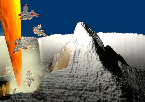
The tip is 500 nm long and a few nanometres wide at its apex. It is attached to a cantilever that scans the surface of the substrate with an accuracy of just 1 nm. By applying heat and force, the tip can remove substrate material based on predefined patterns, rather like a “nanomilling” machine, says Knoll.
The IBM team chose to use organic glass in its proof-of principle experiment because the bonds between the molecules in this material can be easily broken at the temperatures of the tip (300–500 °C).
Alpine sculpture
The new technique is also cheaper than e-beam lithography because it uses less power and can sit happily on a bench top – as opposed to electron-beam machines, which are much bulkier devices. It can be used to make 2D patterns or 3D “sculptures” by successive rounds of etching. Indeed, the team have fashioned a 25 nm high 3D replica of the Matterhorn, the famous Swiss mountain.
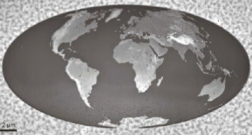
The researchers have also made the tiniest 3D map of the world ever using a tip at higher temperatures of 700 °C. They were able to produce the map in just a couple of minutes.
The team now hopes to commercialize the technology, and also make it widely available to university researchers too. “This will also help to develop the tech further and enlarge its potential applications,” says Knoll told. The researchers also plan to improve the technique so that it can etch even smaller and deeper patterns, while operating faster.
The research is reported in Science.
