Invented 30 years ago, the atomic force microscope has been a major driver of nanotechnology, ranging from atomic-scale imaging to its latest applications in manipulating individual molecules, describe Bruno Schuler, Gerhard Meyer and Leo Gross
The past three decades has seen a revolution in our understanding of nature at the nanoscale. This immense progress owes much to the invention of advanced scanning probe microscopes that let us visualize and manipulate nanoscale objects. The scanning tunneling microscope (STM), which was developed in the early 1980s, achieved an unprecedented spatial resolution comparable with the size of an individual atom. Invented by Gerd Binnig and the late Heinrich Rohrer of IBM Research Rüschlikon in Switzerland, the pair received the 1986 Nobel Prize for Physics for the groundbreaking work. Then, in that same year, Binnig – together with IBM’s Christoph Gerber and Calvin Quate at Stanford University in the US – implemented the first atomic force microscope (AFM). Together, these tools have shaped the trajectory of nanotechnology ever since.
At the heart of all scanning probe microscopes is the probe tip, which scans the surface of a sample using piezoelectric translators. High-resolution maps of the topology and other surface properties can be achieved if the tip is sharp enough and held near to the sample. In contrast to scanning and transmission electron microscopes, which were invented many years earlier, scanning probe microscopes do not require sophisticated electron-focusing optics. The diffraction limits and optical aberrations that plague these and visible microscopes therefore do not apply, meaning that the resolution of scanning probe microscopes is mostly limited by the sharpness of the probe tip.
Importantly, scanning probe microscopes can both image the surface of a sample and carry out various types of spectroscopy; they can even modify surfaces directly. Atoms can be pushed around, for instance, as shown for the first time by Don Eigler and co-workers at IBM Research Almaden in the US in 1990 (Nature 344 524). A decade after this breakthrough, a team from the Free University of Berlin used an STM to dissociate and fuse molecules and thus trigger chemical reactions on individual molecules in a controlled manner, marking an important step towards the synthesis of molecules from atomic building blocks (Phys. Rev. Lett. 85 2777).
The STM and AFM differ in how they measure the interaction between the sample and the tip. The STM is based on quantum-mechanical tunnelling, whereby an electron has a finite probability to pass through the potential barrier between the tip and the sample, which is classically forbidden. The tunnelling current decreases exponentially with the tip–sample distance, resulting in high spatial resolution, but the STM is restricted to small tip heights and also to samples that are electrically conducting.
The AFM, in contrast, relies on measuring the force between tip and sample. Consequently, the AFM is not limited to studying conducting samples and also works extremely well outside vacuum conditions and even in liquids. Moreover, the various interaction forces between the sample and the AFM tip have very different origins and decay lengths. For these reasons, the AFM has become a more widely used tool than its STM ancestor.
The AFM has undergone a number of different physical implementations over the years. Common to each is a cantilever that holds the tip, which is deflected because of the interaction between the tip and the sample. In the first implementation of an AFM 30 years ago, an STM was used to measure the deflection of a metallized cantilever. Later, this approach was superseded by optical-beam deflection, fibre interferometry and piezoelectric detection. Indeed, the particular operational mode of an AFM is chosen depending on the conditions under which the measurement is conducted, the materials being studied, and the properties being investigated. Since the interaction forces between the tip and the sample include components from electrostatic, magnetic, capillary, Van der Waals or chemical forces, in addition to effects caused by friction, mechanical properties and heat conduction, the AFM can provide an enormous range of microscopes and spectroscopes with a plethora of different applications.
Atomic resolution
Some of the most exciting applications of the AFM today demand instruments with the highest possible lateral resolution. For this purpose, an AFM tends to be operated in “non-contact” mode, as introduced in 1991 by Dan Rugar and co-workers at IBM Research Almaden (J. Appl. Phys. 69 668). Unlike the more conventional contact mode, where the tip physically touches the surface and the force on the tip leads to a static deflection of the cantilever, when operating in non-contact mode, the tip and sample never touch.
The interaction between them can still be measured, however, by making the cantilever oscillate and detecting how much its resonance frequency becomes detuned as it moves across a surface. In order to obtain the highest possible resolution, the AFM will also typically operate under extreme conditions: an ultrahigh-vacuum environment leads to atomically defined surfaces with as little contamination as possible, while cryogenic temperatures immobilize molecules on the surface, thus decreasing thermal drift and increasing the stability of the system.
In 1995 Franz Giessibl, now at the University of Regensburg in Germany, used an AFM to obtain atomic-resolution images of the silicon “7 × 7” surface (Science 267 68). Imaging this particular surface at the atomic scale had been the defining breakthrough for the STM 10 years earlier, and achieving it with an AFM proved that the technique had finally caught up in spatial resolution. About a decade after this milestone, however, another great leap forward for the AFM was achieved by Yoshiaki Sugimoto and colleagues at Osaka University in Japan based on studies of the surfaces of semiconductor alloys, demonstrating both elemental sensitivity and atomic manipulation with an AFM even at room temperature (Nature 446 64; Science 322 413). Then, in 2007, Alexander Schwarz and co-workers at the University of Hamburg in Germany demonstrated atomic contrast for the first time by using an AFM to directly detect the magnetic exchange force (Nature 446 522).
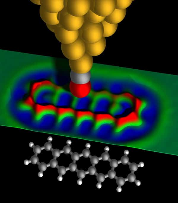
A great advance in high-resolution AFM came even earlier, with the introduction of the “qPlus” sensor in 1998 (Appl. Phys. Lett. 73 3956). This piezoelectric cantilever – based on a quartz-crystal tuning fork – allows oscillation amplitudes smaller than an atomic diameter, which is crucial for measuring short-range forces at the atomic scale. In 2008 Markus Ternes and co-workers at IBM Research Almaden used this detection scheme to slide single atoms across a surface using an AFM and also to directly measure the forces involved (Science 319 1066). The following year, at IBM Research Zurich, the research group of the present authors used a similar set-up to resolve the atomic structure of individual molecules for the first time using an AFM (Science 325 1110). The trick, which we discovered by chance, was to modify the tip itself using atomic manipulation. It turned out that after the pick-up of a single carbon monoxide (CO) molecule by the AFM tip, the resolution on molecules was dramatically increased.
Such tip functionalization is important for several reasons. First, it makes the tip passive and thus stops the molecule under study from being picked up. Second, the CO molecule effectively produces a very sharp tip because of the small atomic radius of the attached oxygen atom. Finally, since the CO molecule is flexible, it may tilt and cause an apparent increase in resolution because chemical bonds appear sharpened and the relative variations caused by bond-order differences are exaggerated (Science 337 1326). The measured force variations corresponding to the interaction between the CO molecule at the tip and the molecule being imaged are on the order of piconewtons (10–12 N). Several other tip functionalizations, for instance using a single xenon, krypton or chlorine atom, have also been shown to achieve atomic resolution. However, because of the stability of CO tips and the apparent sharpening thanks to the CO tilting, CO tips are the most popular to date.
Addressing single molecules
This trick for AFM imaging paved the way for studying the structure and chemistry of individual molecules. It meant that the AFM could be used to identify unknown compounds (Nature Chem. 2 821) and to investigate products formed by on-surface synthesis (Science 340 1434), for instance. Another unique advantage of an AFM for this purpose is that it offers the possibility of studying complex molecular mixtures molecule by molecule. Alternative protocols also allow the charge distribution within a molecule to be mapped, as well as the adsorption geometry to be measured with unprecedented resolution and tiny differences in the bond order to be detected within individual molecules.
Such detailed knowledge about complementary molecular properties is essential for understanding and predicting the reactivity, stability and interaction of molecules with respect to their environment. After all, single molecules and their functionalities are promising for applications in organic photovoltaic devices, molecular electronics and the synthesis of novel compounds.
CO tip functionalization is now widely used in the AFM community to achieve atomic-level resolution where it was not possible before. Recently, for example, an AFM was used to visualize molecular networks based on hydrogen (Science 342 611) and halogen bonding (ACS Nano 9 2574) with atomic resolution, and last year a team used an AFM to resolve the atomic arrangement of metal clusters relevant for fundamental studies of catalysts (Science 348 308). AFMs fitted with CO tips have also turned out to be highly suited for the investigation of graphene sheets and nanoribbons, with recent studies determining the exact atomic termination (Nature Commun. 4 2023), precise position of dopant atoms (Nature Commun. 6 8098) and atomic resolution of graphene edges and junctions (Nano letters 15 5185). The performance of eventual devices based on such 2D materials depends crucially on their exact atomic structure, which an AFM can determine better than any other tool. Moreover, the AFM allows such systems to be atomically modified.
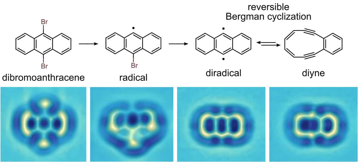
Indeed, the combination of high-resolution AFM with atomic manipulation now offers the unprecedented possibility of custom-designing individual molecules by making and breaking bonds with the tip of the microscope and directly characterizing their products on the atomic scale. Very recently, our group was able to form diradicals by dissociating halogen atoms and then reversibly trigger a ring-opening and ring-closing “Bergman” reaction via atomic manipulation, allowing us to switch and control the molecule’s reactivity, magnetic and optical properties (Nature Chem. 8 220). This offers novel functionalities for molecular-based logic and opens new routes for the creation of designer molecules by single-molecule radical chemistry.
Importantly, a high-resolution AFM offers opportunities to understand and control physical, chemical and biological processes at the level of individual molecules. Ongoing improvements in force sensitivity plus temporal and spatial resolution will push the frontiers in nanoscience further. Perhaps in another 30 years the AFM might be further improved towards an atomic assembler as addressed by Richard Feynman in his famous 1959 talk “There’s plenty of room at the bottom”: a tool that might build arbitrary, 3D atomically precise devices, metamaterials and molecules. Either way, there is no doubt that the AFM will continue to promote discoveries from fundamental physics all the way to chemistry and the life sciences, unravelling nature’s most enigmatic mechanisms at the nanometre scale and beyond.