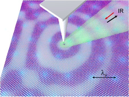
Researchers at the University of California at San Diego (UCSD) are the first to have used infrared nano-imaging to study how surface plasmons (collective oscillations of electrons) propagate in “moiré-patterned” graphene grown on hexagonal boron nitride. The observations, which reveal new collective plasmon modes, could help in the development of advanced plasmonic circuits for novel tunable optical and optoelectronic devices.
Graphene, a 2D honeycomb lattice of carbon first isolated in 2004, boasts a wealth of fascinating electronic properties, many of which come from the fact that it is a semiconductor with a zero-energy gap between its valence and conduction bands. Near where the two bands meet, the relationship between the energy and momentum of an electron in the material is described by the Dirac equation and resembles that of a photon.
These bands, called Dirac cones, enable electrons to travel through graphene at extremely high speeds, which means that graphene-based electronic devices, like transistors, could be faster than any that exist today.
Hexagonal boron nitride (hBN) is an excellent substrate for graphene because the two materials have very similar lattice constants. When graphene is epitaxially grown on top of hBN crystals at a small relative angle, moiré patterns appear. These periodic superlattice structures, which form whenever two similar 2D lattices are precisely overlaid, radically alter the electronic band structure of graphene so that “satellite” sub-Dirac cones appear at the superlattice zone boundaries.
Composite infrared surface plasmons
The researchers, led by Dmitri Basov and Michael Fogler, have now found that new interband transitions in the superlattice mini-bands together with free electrons in the Dirac bands produce composite infrared surface plasmons. “This novel form of collective modes is likely to be generic to other forms of moiré superlattice structures,” explains team member and first author of the study, Guangxin Ni. The experimental observations performed in conjunction with theoretical band structure calculations, were carried out by our colleague Jhih-Sheng Wu at UCSD.
“In such moiré-patterned graphene/hBN heterostructures, the surface plasmons are now composite modes, which is a drastically different situation to that in plain graphene,” he adds. “We also found that the interface between plain graphene and moiré-patterned graphene in our samples acts as a self-assembled “plasmonic reflector”. Such features are essential elements for nanoplasmonic circuits and ‘transformational plasmonics’, which allows us to tune plasmonic fields at will.”
The team, which includes researchers from the National University of Singapore, Shanghai Institute of Microsystem and Information Technology and Ludwig-Maximilians University and Center for Nanoscience in Munich, is now busy trying to extend its approach to the terahertz and far-infrared parts of the electromagnetic spectrum. “Composite plasmons should be even more robust in these regimes,” Guangxin tells nanotechweb.org.
The research is detailed in Nature Materials 10.1038/nmat4425.
- This article was first published on nanotechweb.org


