The observation of optical gain - a key feature of all laser systems - in silicon nanocrystals could revolutionize the semiconductor and telecommunications industries, although further work is needed to develop a practical silicon laser.

Devices made from silicon dominate the microelectronics industry, so silicon should be the material of choice for anyone designing new electronic devices that will be integrated with microelectronic circuits. This also applies to the optoelectronic devices that act as gateways between the electronic realm and the worlds of photonics and optical communications. Most optoelectronic components – such as waveguides and modulators – can be made from silicon, but a completely silicon-based system has remained elusive because there is a crucial missing link: a silicon light source.
A silicon laser made using “conventional” silicon-manufacturing technologies would be a disruptive new technology that could have a massive impact on the future of the semiconductor, IT and telecommunications industries. However, the electronic structure of silicon means that it is not good at amplifying light – a key characteristic of any laser medium. Now Lorenzo Pavesi of the University of Trento in Italy, and colleagues at Trento and the University of Catania, have taken a significant step towards a silicon laser by demonstrating light amplification in silicon (L Pavesi et al. 2000 Nature 408 440). However, several technical challenges must be overcome before this breakthrough can be transformed into a practical silicon laser.
Making the connection
Microelectronic systems have now reached the stage where their performance depends on the connections between the different chips and devices, rather than on the chips and devices themselves. Industry experts believe that within a decade the same problem will apply at the level of single chips. As semiconductor systems get ever smaller, the metal tracks currently used to connect the different components on a single chip will suffer increasingly from problems such as lack of speed and unacceptable levels of power dissipation.
Optical connections are an attractive alternative because they promise to eliminate these potential problems. However, the practical implementation of optical connections presents a major challenge, and the key problem has always been the lack of a semiconductor laser that is fully compatible with silicon microelectronics.
The electronic structure of silicon does not allow it to emit light readily. In a so-called direct-band-gap semiconductor, such as gallium arsenide, a photon is emitted when an electron from the conduction band falls into the valence band and “recombines” with a positive hole. The wavelength of the photon is determined by the energy difference or “band gap” between the conduction and valence bands.
Silicon, however, has an “indirect” band gap: this means that the minimum in the energy of the conduction band and the maximum in the energy of the valence band occur at different momenta. Therefore, electrons and holes can only recombine if a lattice vibration – known as a phonon – with the correct momentum is available. This makes the emission of a photon much less likely.
One way to force silicon to emit light is to illuminate it with a separate light source: this excites electrons from the valence band into the conduction band, from where they fall back down to the valence band – sometimes emitting photons in the process. This phenomenon is known as photoluminescence. Bulk silicon has a photoluminescence efficiency of much less than 0.01%. Moreover, the light is emitted at only one wavelength in the infrared part of the spectrum.
In 1990 Leigh Canham at the DRA Malvern laboratory in the UK showed that, under certain conditions, silicon can emit light efficiently, even in the visible part of the spectrum. This was first achieved using porous silicon, which has a band structure that is slightly different from bulk silicon. Today we know that very efficient (i.e. above 1%) photoluminescence can be achieved in many materials if they incorporate quantum dots or wires made of silicon.
Measuring just a few nanometres, these structures are known as nanocrystals and they have unusual electronic properties because their band gaps are wider than those of the materials from which they are made. In particular, electrons and holes become “localized” inside the nanocrystals, which increases the chance that they will recombine and emit photons. Competing recombination processes that do not result in the emission of light can also be suppressed by passivating the surface.
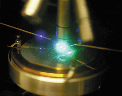
Now Pavesi and colleagues have produced optical gain in silicon nanocrystals made by implanting silicon in thin silicon-dioxide layers grown on silicon wafers. The nanocrystals, which measured about 3 nm across, are embedded in a crude waveguide. A laser then excites the structure, generating electrons and holes in the nanocrystals that recombine to emit light with a wavelength of about 800 nm, which lies between the visible and infrared regions of the spectrum. They reported amplification factors or “net modal gains” of 100 per centimetre in their structures. This means that spontaneous emission in the device is amplified by a factor of [l/(g – a)](e(g – a)l – 1), where l is the distance over which amplification occurs and g – a is the net modal gain.
In a different experiment, the “material gain” – the gain or amplification that would be measured if all of the beam passed through the gain region – reached 10 000 per centimetre. This is comparable with the best results for indium arsenide and other quantum-dot systems. This totally unexpected result is due to the very large concentration of nanocrystals, which more than offsets the smaller gain cross-section of each nanocrystal.
The researchers propose that the recombination involves silicon-oxygen double bonds located at the interface between the silicon nanocrystals and the oxide matrix. In their three-level model, pumping takes place from the valence band to the conduction band within the nanocrystals. The electron is then captured by the silicon-oxygen double bond, and emission occurs when the electron in the double bond recombines with the hole that is still in the valence band of the nanocrystal. Whether this model is correct remains to be seen.
Towards a practical device
So how can we exploit this phenomenon to make a working silicon laser? A laser consists of an optical-gain material sandwiched between two mirrors to form an “optical cavity”. The mirrors direct the emitted light back into the cavity to produce more light and, ultimately, create an intense, coherent beam. To achieve laser action, the optical gain must be high enough to outweigh the losses from the cavity.
How soon will we be able to make a silicon laser? First, Pavesi’s findings must be reproduced, and other groups are likely to take up the challenge soon. Next we must establish the conditions for maximum optical gain and optimize the device. It is also important to realize that Pavesi’s group achieved optical gain in silicon by exciting it with light, whereas any practical device will need to be driven electrically. The final hurdle in the race for a silicon laser could well be the challenge of finding a way to inject electrons or holes into silicon nanocrystals using an electrical current – and so far that has not been easy.
* A group at the University of Illinois claims to have seen evidence for the stimulated emission of blue light from individual silicon nanoparticles (see Physics World January p7, print version only)


