Metal chalcogenides like MoTex have been used in various electronics devices because of their intrinsic semiconducting properties, since the exact nature of their electronic structure can be tuned from semiconducting to metallic based on their atomic arrangement. Scientists from the University of Texas at Dallas have discovered a way of inducing this electronic transition simply by heating the 2H-MoTe2 semiconducting phase in a vacuum to produce metallic Mo6Te6 nanowires. This simple synthesis technique could help the development of a new generation of tunable semiconductor devices.
Semiconducting materials are used in most electronic devices, and the ability to tune their properties through simple techniques is the holy grail of material synthesis. By identifying a new, conducting nanowire phase of this material family, lead researchers Robert M Wallace and Moon J Kim have helped integrate these materials into the fabrication of MoTex-based electronics.
Making the nanowires
Wallace and Kim observed the phase transition from layered 2H-MoTe2 to the Mo6Te6 nanowire (NW) phase after heating 2H-MoTe2 to approximately 450 °C in vacuum. The new NWs were stable at room temperature and after reheating because the ratio of Te/Mo significantly decreases to accommodate the phase transition. Other synthetic techniques induce the 2H (semiconducting) to 1T’ (metallic) transition under much higher temperatures, typically above 900 °C. However, since such high temperatures were not used in this study, no 1T’ phase was observed. The metallic character was therefore attributed to the new NW phase.
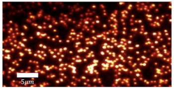
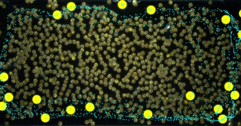
The researchers observed the nanowire phase transition by scanning transmission electron microscopy (STEM), providing beautiful images and videos of the reaction propagation in the crystals. The phase change appears to initiate at the surface of the 2H-MoTe2 crystal where Te desorption is highest, and can easily be modified with annealing time or temperature. This transition is atomically sharp with a well-defined interface between the two phases. The researchers characterized this new phase showing the 1D chain of Mo-Te NWs consisting of infinitely staggered Mo3Te3 units.
Looking at the electronic structure
Interestingly, scanning tunnelling microscopy (STM) and X-ray photoelectron spectroscopy (XPS) showed that the NW bundles were metallic in character, but density functional theory (DFT) simulations showed that may not be the case for an isolated NW. When the NWs exist in bundles, the conduction band is partially occupied, creating a band gap equal to zero. However, when the NWs are isolated the calculated band gap is approximately 0.3 eV, showing the importance of the surrounding electronic structure in the crystal. The reported NWs from this synthesis procedure exist solely in bundled clusters and were therefore only observed as a metallic conductor.
The researchers clearly demonstrated the phase transition from the layered 2H-MoTe2 phase to Mo6Te6 nanowire bundles preferentially forming at the surface of the crystal. They also showed that the NWs could have both a semiconducting and metallic electronic structure based on the intrinsic conduction network that exists both in a single wire and in bundled wires.
Ever since the discovery of 2D graphene and 1D carbon nanotubes, low-dimensional materials have inspired innovation and stretched the frontiers of various fields of materials science. Metal chalcogenides are on a similar path, with first the introduction of the 2D layered metallic 1T’ phase and now the Mo6Te6 nanowires. Clearly, this work will have significant impact on future material design.
More information can be found in Advanced Materials.