Since the first lasers appeared nearly 50 years ago, scientists and engineers have dreamed about creating all-optical circuits in which electrons are replaced by photons. While information is easily transmitted via light using optical fibres, switching and processing the information still rely on converting photons to electrons and then back again — which is a slow and power hungry process.
Unfortunately we are still far from seeing all-optical — or “photonic” — circuits in desktop computers and other everyday applications because these circuits require light to be manipulated in nanometre-sized spaces, something that is very difficult to do. Moreover, the efficient all-optical switching of light beams, which allows energy from one beam to amplify another, usually requires large photonic crystals.
Now, Vahid Sandoghdar and colleagues at ETH Zurich have made what they say is the world’s smallest optical transistor ever — from a single dye molecule. The device, which works by weakening or amplifying a “source” laser beam depending on the power of a second “gating” beam, could bring all-optical circuits and optical computing a step closer.
‘Simple’ operation
“By controlling the degree of attenuation and amplification via the power in a second gating laser beam, we have demonstrated the smallest optical transistor to date,” Sandoghdar said.
The operating principle is simple, he says: when the molecule is placed in an excited state by the gate beam, it can emit a photon, therefore amplifying the source beam.
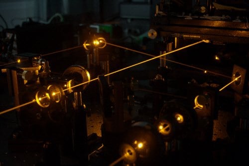
The key to making the new optical transistor is the tight focusing of light onto a single molecule at ultra-low temperatures. This focusing provides strong light-molecule coupling that allows the molecule to affect the laser light.
Although strong coupling has been achieved before, it had taken place in optical cavities, in which interactions can be enhanced. However, even the smallest optical cavities are larger than about a micron in size, which means that devices cannot be made any smaller than this.
High-density packaging
By contrast, the cavity-free ETH Zurich experiments could lead to high-density packaging of nanometre-sized all-optical transistors. Theoretical calculations by the team also show that it should be possible to build complex circuits where many single emitters are coupled to tiny waveguides that carry optical signals on a chip.
“And although our experiment was performed with conventional laser beams, the set-up also works for non-classical light beams at the single photon level,” explained Sandoghdar. “This means that quantum information processing will be possible.”
The work was reported in Nature .


