Researchers have discovered a novel way of switching the polarization of an ultrathin ferroelectric material. The mechanism, dubbed “slidetronics” because it occurs when adjacent atomic layers in the material slide across each other, could be an efficient alternative way of controlling tiny electronic devices.
Being able to switch electrical polarization over small areas is key for modern technologies such as hard disk drives that store and retrieve large volumes of information. The dimensions of individually polarizable domains (that is, regions with a fixed polarization) within the silicon-based devices commonly used for information storage has dramatically decreased in recent years, going from roughly 100 nm thick to the atomic scale.
The main challenge to making these structures even tinier is overcoming long-range interactions between neighbouring domains, which tend to cause the polarization of individual domains to align. Surface effects also become more important as domain sizes become smaller because the surface-to-volume ratio increases.
Breaking the symmetry
To address these difficulties, researchers have begun to explore alternatives to silicon in the form of two-dimensional materials such as hexagonal boron nitride (h-BN) and the transition metal dichalcogenides (TMDs). These materials, which can be made just one atom thick but remain crystalline with a well-defined lattice and symmetry, are made up of stacked layers held together by weak van der Waals (vdW) interactions. However, polarization in naturally-grown h-BN and TMDs is limited because it is energetically favourable for these materials to adopt a so-called “centrosymmetric” vdW structure that looks the same when the crystal is flipped.
Researchers led by Moshe Ben Shalom at Israel’s Tel Aviv University have now broken this undesirable symmetry by controlling the angle, or twist, between two stacked h-BN layers. In the process, they discovered a multitude of permanent and switchable polarizations – oriented perpendicular to the material’s surface – at the interface between the layers.
“The stacking arrangement that breaks the symmetry and hosts polarization is one out of five possible configurations in bilayer h-BN,” Ben Shalom explains. “We divided these into two groups: ‘antiparallel’ and ‘parallel’ twist orientations.”

In the optimal antiparallel (AA’) configuration the nitrogen atoms of one layer and the boron atoms of the adjacent layer overlap fully. In the unstable parallel (AA) orientation, bulky nitrogen atoms are forced to sit atop each other, producing a repulsion between the layers. To solve this problem, the layers shift laterally, sliding past each other until they can form a metastable stack in which only half of the atoms overlap with each other (the AB configuration).
“A beautiful ‘Moiré’ pattern”
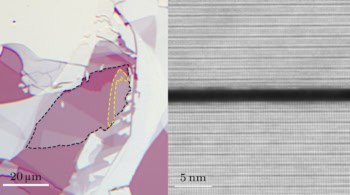
In the experiments, team member Maayan Vizner Stern used sticky tape to separate individual atomic layers from a multilayer bulk crystal of h-BN and transfer them onto a flat surface. (Andre Geim and colleagues at Manchester University in the UK used a similar technique to isolate layers of graphene from bulk graphite in 2004.) Stern then picked up the layers using a microscope slide covered with a soft, transparent polymer and placed one crystalline layer on top of another such that the lattices of both were oriented parallel to each other in an AB stack.
“The artificially stacked parallel structure we made results in a tiny interlayer shift with only half of the nitrogen or boron atoms eclipsed and is not symmetric when flipped,” Ben Shalom tells Physics World. “What is more, when we scanned the local surface potential with the tip of an atomic force microscope, we observed a beautiful ‘Moiré’ pattern of triangle domains in which the (out-of-plane) polarization flips.”
Domain wall sliding
Most importantly, the researchers found that scanning an electrically-biased tip across the surface makes the domain walls in the material slide across each other. This sliding allows the polarization orientation to be switched locally, as desired.
‘Twistronics’ tunes 2D material properties

Thanks to extensive numerical calculations by team member Wei Cao, the researchers were able to follow how the charge on the different lattice sites in h-BN reorders due to the broken symmetry. Led by another member of the collaboration, Eran Sela, they used this information to build an intuitive model that explains the phenomenon. According to Ben Shalom, it turns out that there is a competition between the Coulomb attraction and the vdW forces in the pairs of fully-eclipsed atoms versus the separated pairs. This mechanism could be used to predict similar polarization behaviour in other hexagonal diatomic crystals.
Ben Shalom observes that the presence of such a stable polarization in a two-atom-thin system could be very useful for efforts to miniaturize non-volatile electronics devices. At the atomic scale, the electrons can efficiently quantum-tunnel across the two layers, and this tunnelling mechanism can be used to rapidly read and write the polarization. Looking longer term, he suggests that the lateral mechanical sliding and perpendicular polarization switching mechanisms observed in this study, which is detailed in Science, may even have applications beyond what we can predict today.