Physicists in the Netherlands are the first to show that spin-polarized electrons can be injected into silicon at room temperature. The team injected the electrons into both p-type and n-type silicon and measured how long the polarization lasted. Although the lifetime was shorter than expected the physicists believe it is long enough to support the development of spintronics devices.
The team are also the first to detect spin-polarized electrons in p-type silicon at any temperature.
The intrinsic spin of the electron can either be “up” or “down”, and this property could be used to store and process information in spintronic devices. Such circuits could be smaller and more energy efficient than conventional electronic circuits because they would rely on flipping spins rather than switching charge.
Silicon is the material of choice for conventional electronic circuits and physicists already know that it can support and transport spin-polarized electrons at temperatures lower than about 150 K. The challenge is to boost this to room temperature so that practical devices can be made from silicon.
Room temperature injection
Now Ron Jansen and colleagues at the University of Twente are the first to show that spin-polarized electrons can be injected into silicon at room temperature. The team began by depositing three insulating oxide contacts onto a piece of silicon, and then topped each contact with a magnetic metal electrode.
The metal is magnetized parallel to the surface of the silicon and a constant current of electrons is made to flow out of one electrode, through the silicon and into a second electrode. The resistance of the silicon is determined by measuring the voltage between the first (source) electrode and the third electrode.
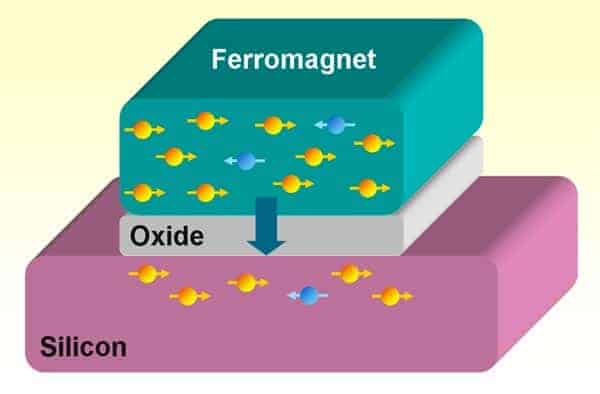
The electrons in the magnetic electrode are polarized, with most spins pointing along a specific direction. Some of this polarization is preserved as the electrons tunnel across the oxide and into the silicon leading to an accumulation of spin in the region under the source electrode (see diagram above).
Change in resistance
Electrons are fermions and tend to avoid each other if their spins point in the same direction. This means that the resistance of the contact interface increases as more polarized electrons accumulate in the silicon. However, if a magnetic field is applied perpendicular to the polarization, the spins precess about the field. This reduces the spin accumulation and the resistance of the contact interface.
Jansen and colleagues observed this effect by measuring the voltage (and therefore resistance) across the two electrodes while changing the strength of the applied field. The overall change in resistance allowed them to calculate the spin accumulation in the silicon – about 5% at room temperature. They were also able to determine the mean lifetime of a spin in silicon by studying the shape of the voltage versus applied field curve.
In n-type silicon this lifetime was about 140 ps in n-type silicon and 270 ps in p-type. This is shorter than electron spin resonance (ESR) measurements, which suggest lifetimes of about 1 ns at room temperature for the n-type silicon.
Long enough?
However, a lifetime of about 200 ps should allow a spin to travel a few hundred nanometres through a spintronic device before decaying – and Jansen says that in principle this is more than enough to make spintronics circuits that are tens of nanometres in size and operate at frequencies of 10–100 GHz.
Ian Appelbaum of the University of Maryland described the short lifetimes as “disappointing [but] not entirely surprising: this may be caused by high doping and the presence of interfaces”. Appelbaum told physicsworld.com that, while the injection of spins into room temperature silicon is important, the researchers have not shown that spins are transported through the material – the latter being crucial for any practical spintronic device.
Jansen and his team are now planning to study the transport of spins between electrodes as well as studying how the spin lifetime is affected by doping, temperature and the interface between the silicon and the magnetic metal.
David Awschalom of the University of California Santa Barbara said that the Twente structure could “serve as a ‘spin laboratory’ within which one may begin to optimize electron spin transport and control in this material”.
The work is reported in Nature.


