Photonics-based computing uses less energy and can transmit data faster than conventional approaches, but the costs of manufacturing silicon integrated circuits with embedded photonic elements have held back progress. Scott Jordan outlines how improved optical positioning technologies could help

The world’s appetite for data is growing exponentially, driven by applications ranging from social networks and streaming media to genomics-driven medicine and the proliferation of connected devices within the “Internet of Things”. The growth in mobile computing is especially stark. According to the United Nations’ telecommunications agency, by 2013 the number of mobile phone subscriptions was already approaching the number of humans on Earth. Landline telephones, in contrast, have never reached more than 25% of the global population.
The bountiful opportunities provided by these technologies and services – and by whatever comes after them – ensure that people will continue to find new ways for data to connect, entertain, inform and help us. But this increased data use comes at a cost. In 2009 Google revealed that a single Internet search consumes about 1 kJ of energy. By 2016 industry experts estimated that the world’s data centres – massive monoliths of servers and switches – were consuming almost 40% more electricity than the entire UK. The figure has likely grown since then, as increases in data volumes have so far outstripped improvements in efficiency.
Another challenge for our data-intensive world is that even at the level of consumer devices, data rates are starting to exceed the capability of conventional interconnect technologies. For example, the extraordinary pixel density and high frame rates of the latest high-definition televisions are rendering conventional copper HDMI cables increasingly ineffective. Even over the relatively short distances found in home entertainment systems, the degree of signal degradation in such cables is significant.
The central problem here is that conventional, electronic data systems require wires to be charged and discharged in order to send a bit of data from point A to point B. Even in the microscopic wires found inside CPU and RAM chips, this charge-discharge cycle takes both energy and time. As David Miller, an applied physicist and electrical engineer at Stanford University in the US, has pointed out, most of the energy used in information processing goes towards communications, not logic. Even at the gate level, the main driver of energy dissipation is the capacitance of the wires being charged and discharged, which amounts to about 200 attofarads (10–18 F) per micron of wire. At the data-centre level, the largest server farms may consume an entire power plant’s worth of electricity, so the efficiency of server-to-server interconnects poses serious sustainability issues.
Many of these issues would be substantially mitigated if cables and switches were configured to communicate using photons rather than electrons. The promise of photonics in computing and communications actually extends far beyond this, encompassing new possibilities for logic and processing as well as some approaches to quantum computing. Those applications lie in the near- to mid-term future, but photonic interconnects are available today, with advantages including scalability, capacity, parallelism, longer link-lengths and speed. Even consumer applications benefit. Optical HDMI cables can now support high frame rates for displays 4000 or 8000 pixels in width (and beyond) over commercially useful cable lengths, and optical USB and Thunderbolt implementations are emerging for data rates of 40 Gbps and upward.
Manufacturing these photonic devices isn’t easy, however. Sure, the process begins with the same silicon wafers that have been ubiquitous in microelectronics for decades, and it uses many of the manufacturing tools found in standard semiconductor fabs to print optical components and circuitry onto wafers alongside (or instead of) microelectronic elements. However, photons fundamentally do not obey the same physics as electrons. Guiding a photon from one element to another inside a packaged “chip” is not as simple as soldering the two together. For one thing, alignment tolerances are much more exacting. Whereas connecting a wire to a contact-pad on a chip involves aligning the components to within a few tens of micrometres of the correct position, connecting an optical fibre to a photonic chip can require three orders of magnitude more precision. Fortunately, thanks to ingenious device engineering and some groundbreaking micro-robotic industrial automation technology, we are well on our way to overcoming these challenges, bringing high-throughput photonic interconnects into the mainstream.
Precedents for progress
The challenges involved in manufacturing systems that use photons to transmit information are not new. In fact, they date at least as far back as the late 1990s, when photonics technology was first deployed on a grand scale to replace satellite links in long-distance telecommunications. At the time, the task of sending light from then-novel laser diodes down a single-mode optical fibre required the positions of both components to be laboriously adjusted before the laser’s light was efficiently coupled into the fibre. An analogue technology called a gradient search was a partial solution, enabling the positioning system to quickly reach an optimum transmission value (at least for fibres with a smooth modal profile). However, the positioning systems themselves had significant limitations. They were often fragile, with limited travel ranges and a tendency to drift out of alignment – not good qualities for systems being deployed in industrial environments. The problem was ultimately solved by developing a digital version of the gradient search and deploying it on industrial-class motion hardware that had already proven its worth in semiconductor manufacturing. The combination provided a path forward for manufacturing robust hardware for optical fibre interconnections.
Today’s photonic data devices are significantly more sophisticated and complex. Thousands of photonic integrated circuits (ICs) can be minted on a single wafer, offering the tantalizing potential for processing multiple channels of light at once, increasing capacity and speed. Photonics ICs today routinely integrate both multi-channel and multi-wavelength structures, with inputs and outputs arranged in arrays that enable each device to process and carry multiple channels of information.
In some respects, though, the challenge of making these circuits “talk” to each other is the same as it was for telecoms fibres. All of the chip-level photonic inputs and outputs need to be coupled to other elements, including optical fibres, fibre arrays, waveguide-based structures, laser diodes and bulk elements such as lenses and gratings, as well as other chips. Many of these couplings require meticulous alignment not only in the sensitive transverse plane (by convention referred to as the “XY” plane) but in other degrees of freedom. Importantly, an array of photonics devices must be precisely oriented not only in the XY plane but also in the theta-Z direction, and often in other degrees of freedom (DOFs), too.
Another complication is that the necessary alignment can only be performed actively – by measuring the actual coupling of light into the fibre. This is because the machine-vision approaches commonly deployed to determine device positions during assembly cannot resolve spatial tolerances of tens of nanometres, and passive-alignment approaches (such as precision V-grooves, in which fibres are glued in place) typically require impractical device replication tolerances.
In principle, the 1990s-era digital gradient search would still work for aligning the optical components in silicon photonics. In practice, however, the number of array elements involved, combined with the need for multi-DOF optimization, means that the process of finding a globally optimal alignment is not straightforward. Moving a certain component in the theta-Z axis, for instance, will inevitably cause it to de-align in the XY plane due to the mechanical rotation axis not being precisely coincident with the optical axis.
This problem has often been solved using a looping approach: you align the component in XY; make a small theta-Z improvement; go back and re-align in XY; and then iterate until the result is satisfactory. Looping is also deployed to optimize devices (such as the short, multimode waveguide structures common in silicon photonics) that exhibit interactions between channels and between inputs and outputs. In this case, you start by optimizing the input, then optimize the output – except now the input is no longer optimized, so you loop until you achieve a consensus optimum. Once the optimization process is complete, digital gradient search technology can track the elements’ alignments, ensuring that they stay optimized in the face of drift from thermal changes and the stresses involved in curing glued elements.
Killing off the loops
There’s just one catch: looping is far too slow to be practical for testing and later assembling the thousands of devices from each wafer. To understand why, consider the early stages of wafer manufacturing. As in conventional microelectronics manufacturing, the cost of minting a silicon photonics wafer constitutes only a small part of the finished price of a packaged chip. Since wafer yields are by no means 100%, it makes good economic sense to discard faulty devices before they reach the packaging phase, where costs are considerably higher.
In microelectronics manufacturing, this quality-control process is carried out using specialized tools called wafer probers that subject each chip to contact from precise, needle-like electrodes that stimulate it and observe its response, often via racks of sophisticated instruments. To carry out the same tests on a photonic chip, however, it is not enough just to make electrical contact. Light must also be coupled into and out of the chip’s embedded photonic circuitry, and the chip’s performance measured by optical means. Array elements pose special challenges, since the devices must be rotated into precisely matching orientations as well as translated into tight transverse alignment. Traditionally, optimizations of this sort needed to be performed in a stepwise fashion, with angular adjustments interleaved with transverse re-alignments to compensate for any mismatch between the optical and rotational axes. This could take several minutes – an unacceptable (and uneconomical) length of time, given that each wafer can contain thousands of silicon-photonics chips.
Recently, a solution has emerged in the form of a new approach to digital gradient search that enables industrial positioners to perform gradient searches across multiple channels, inputs and DOFs at the same time. Instead of iteratively making small theta-Z motions interleaved with XY corrections over a span of perhaps minutes, this technology can perform the XY and theta-Z alignments simultaneously, using two gradient-search processes in parallel. This parallel digital gradient search (PDGS) approach can be scaled up to the full six degrees-of-freedom for each device, and multiple positioners can work cooperatively on multiple inputs and outputs of a device even if there are interactions between the inputs, outputs and channels.
Thanks to PDGS, the minutes-long, serial process of looping (for example) the XY and theta-Z alignments of an array device reduces to only a second or so – a time savings of 99%. The parallelism of the technology also means that the overall process time is almost independent of the number of adjustments performed. This is significant because in manufacturing (as in so many things), time is money. It is no surprise that manufacturers and users of wafer probers were the first to incorporate micro-positioning robots that use PDGS, with the first implementations in 2016. The microrobots have also been implemented in other areas of manufacturers’ assembly processes, such as aligning chips and other components together in their packages. Some manufacturers have even instituted specialized test tools for re-validating the health of the chips at intermediate steps in the packaging process. This parallel process has been implemented within the firmware of the industrial-class, six-DOF hexapod microrobots and other precision mechanisms used in manufacturing silicon photonic devices, transforming the unfavourable economics of the silicon photonics industry.
Parallelism beyond silicon
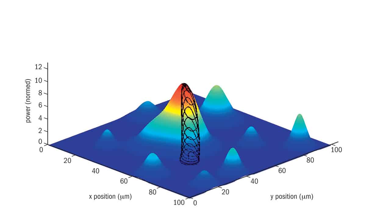
When assembling and testing silicon photonics devices, the parameter being optimized is almost always optical power. However, many other relevant metrics also exhibit a similar sort of roughly hill-shaped optimization trend, and PDGS does not require its inputs to have a purely Gaussian profile (which is a good thing, as silicon photonics devices rarely produce light beams with clean Gaussian profiles). Secondary maxima or “foothills” around the main peak are no problem, as the main mode can usually be selected by performing an area scan. A classical version of this would be a raster scan that sweeps over a defined area, but the microrobots implement a considerably faster approach in the form of a vibrationless sinusoidal or spiral area scan built into the firmware at the command level (see image on p31). This allows the main coupling peak to be identified, ensuring that the gradient search locks onto and tracks the main mode.
This opens the potential for applications of PDGS unrelated to silicon photonics. In laser manufacturing, for example, bulk optics are aligned to a mutual optimum based on various parameters of the output beam. This can be a time-consuming process, so automating it promises significant rewards in terms of yield and production throughput. Cameras are another example. Billions are manufactured every year, largely driven by the world’s demand for smartphones, by the smartphone industry’s steady progress in camera quality and by novel applications such as facial mapping. Each generation of phones integrates more cameras per handset, to the extent that smartphone demand could plummet 50% (something that is not going to happen, I hasten to add) and yet smartphone manufacturers would still require more cameras in 2019 than they did in 2015. Camera adoption in cars and trucks is also skyrocketing, propelled by rapid adoption of safety technologies and autonomous driving capabilities.
With more optical devices of greater sophistication being manufactured each year, the applications of PDGS will continue to expand. By giving nanoscale eyes to microrobots, this technology makes it possible to optimize the position of multiple optical elements in both silicon photonics and other areas of manufacturing – thereby keeping precision positioning up to speed with new chapters being written in computing, imaging and many other areas of photonics technology.
- Enjoy the rest of the 2019 Physics World Focus on Optics & Photonics in our digital magazine or via the Physics World app for any iOS or Android smartphone or tablet.