Researchers at Stanford University and the University of California, Davis, in the US are reporting on the first experimental evidence for ballistic thermal transport across thin films of van der Waals layered semiconductors. The unexpected result will have implications for thermal management in thin-film 2D electronics.
Layered semiconductors, like the molybdenum disulphide studied in this work, are highly anisotropic because of weak van der Waals interactions between the material layers. They conduct heat poorly in the direction normal to the layers as compared to along them.
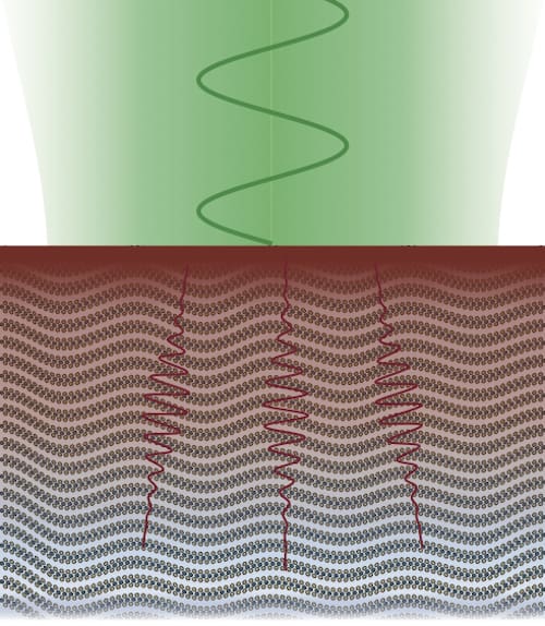
“The ability of a material to conduct heat is directly related to how far thermal vibrations (phonons) in it can travel without decaying, and is measured by their mean free path,” explains Aditya Sood, who is co-lead author of this study. “In our work, we have shown that even though these layers are weakly bonded and conduct heat poorly in the film-normal direction, the mean free paths of thermal vibrations are, surprisingly, still quite large. This means that heat is not transported through localized oscillations of the layers, but through coherent vibrations that travel long distances across hundreds of layers before decaying.”
“It is generally thought that the weakly bonded layers vibrate in a decoupled manner when heat flows across the material, but our result suggests otherwise,” he adds.
The result will have implications for thermal management in thin-film 2D electronics. “While the thermal coupling of single-layer 2D materials is limited by their interfaces, we have found that few-layer 2D materials have a ballistic phonon resistance, quantified here for the first time,” says co-team leader Eric Pop.
The finding could be exploited to make materials with tuneable or ultra-low thermal conductivity by inserting defects between the MoS2 layers, because these could impede the flow of ballistic phonons. “Indeed, we have already demonstrated an application of this phenomenon recently by engineering a thermal transistor based on lithium intercalation in MoS2 thin films”, adds Sood.
Ultrafast thermal metrology
In their present experiments, the researchers used an optical technique called time-domain thermoreflectance, which can sensitively measure the thermal properties of thin films down to nanometre thickness. “We heat up our film with short pulses of laser light and monitor the temperature at the top surface by measuring its reflectivity as the heat from each pulse diffuses through the sample,” explains Sood. “By analysing how fast this cooling occurs (typically within nanoseconds), we can determine the thermal conductivity of the film.”
Grain boundaries limit heat flow in diamond
The team measured the film-normal thermal conductivity of MoS2 films with different thicknesses and found that the conductivity decreases with decreasing thickness. “Thanks to detailed atomistic calculations performed by our colleagues at UC Davis, we realized that this effect was in fact a direct consequence of the ballistic transport of thermal vibrations with mean free paths longer than the film thickness,” Sood tells Physics World. “These modes cannot carry much heat because of strong scattering at the film boundaries, which leads to an overall suppression in thermal conductivity.”
It is this boundary scattering of ballistic phonons that imposes a lower limit on the temperature increase in a device, he says.
The researchers, co-led by Ken Goodson and Yi Cui at Stanford and Davide Donadio at UC Davis, say they would now like to leverage the effects they have observed to engineer synthetic layered materials with extremely low conductivity. “As mentioned, inserting layers of a second material with a different atomic mass should result in scattering of ballistic phonons, leading to a dramatic suppression in heat transport,” explains Sood. “Such artificial solids could have exciting applications as thermal insulators on spacecraft, for example.”
The present study is detailed in Nano Letters 10.1021/acs.nanolett.8b05174.


