Physicists in the UK have found a way to overcome a major barrier blocking the use of graphene in electronic devices – how to prevent current leaking through a device when it is switched off.
Graphene is a sheet of carbon just one atom thick and has a number of unique electronic and mechanical properties that mean it could be used in electronic devices – at least in principle. There are, however, many challenges that must be overcome before commercial applications are possible.
Graphene is an extremely good electrical conductor, but its extreme conductivity is also a problem because devices made from the material remain conducting even when switched off. This not only wastes power, but also means that such devices cannot be packed onto computer chips because the electric current running through the graphene would melt the chips almost immediately.
Graphene is a semiconductor, but unlike familiar materials such as silicon, graphene has no energy gap between its valence and conduction bands. Such a band gap allows a semiconductor to switch the flow of electrons on and off. Researchers have proposed various schemes to overcome this problem – for example by using nanoscale ribbons or quantum dots, or chemically modifying graphene to make it semiconducting. Although both schemes work in principle, opening a band gap in graphene in this way also damages the material so much that finished devices no longer show either ballistic transport or high electron mobilities.
A layered approach
Now, Leonid Ponomarenko and colleagues at the University of Manchester have taken a step forward in overcoming this problem by making a new type of transistor from graphene that contains layers of boron nitride or molybdenum disulphide sandwiched between graphene sheets. The team doing the work also includes graphene pioneers Konstantin Novoselov and Andre Geim.
The layers act as vertical tunnelling barriers that minimize current leakage – even at room temperature. Called a vertical field-effect tunnelling transistor, the device is the first ever made from graphene that can be properly switched on and off – despite the absence of an energy gap in the material’s band structure.
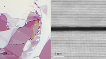
The transistor is made of two graphene sheets sandwiched together with atomically thin insulators such as boron nitride (BN) or molybdenum disulphide (MoS2) that act as barriers for electrons tunnelling from one layer of graphene to the next. The advantage of this type of structure is that the current flowing perpendicular to the layers of the insulating material – that is, the tunnelling current – can be controlled with an external electric field. “Technically, this is because the electrons induced in the graphene by the external field have a higher probability of tunnelling and the number of such electrons increases with the field,” explains Ponomarenko.
Although any insulator can be considered as a tunnelling barrier, it is only when the barrier is a few atoms thick that the tunnelling current can be easily measured. BN and MoS2 are ideal for use in this respect because extremely thin flakes of the materials can be produced using the same “sticky tape” method used to obtain graphene.
Unique feature
The device works thanks to a unique feature of graphene whereby an external voltage can strongly change the energy of the tunnelling electrons, says Ponomarenko. “I think our work now opens the way to creating graphene integrated circuits,” he says.
“The demonstrated transistor is important but the concept of such layer assembly is probably even more so,” adds Geim. Novoselov agrees: “The tunnelling transistor is just one example of the inexhaustible collection of layered structures and novel devices that could now be created by such assembly.”
The team says that it will now look at whether graphene can be combined with other 2D materials. “It will also be important to know how our tunnelling transistors behave when their lateral size is reduced to the nanometre scale and to find out the highest frequencies at which the devices can operate,” says Ponomarenko.
The research is described in Science.