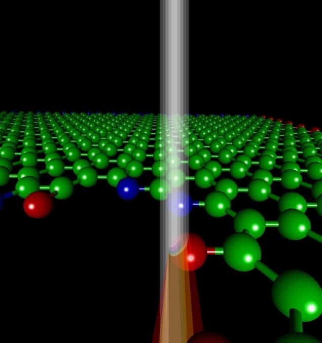
The electronic properties of nanodevices depend strongly on structures just a few atoms in size, so being able to identify individual atoms and their electronic states is becoming increasingly important as devices shrink. Researchers in Japan have now obtained electronic spectra from single carbon atoms in a sheet of graphene using an electron microscope equipped with a tiny probe. Unlike previous methods it does not damage samples – and could be used to explore the local electronic structure in a variety of materials.
As electronic devices become ever smaller, their properties can be very different from their larger counterparts. As a result, device designers need new methods to characterize devices on an atomic scale. For example, graphene (a sheet of carbon atoms just one atom thick) is promising for making future nanoelectronic devices thanks to its unique electronic and mechanical properties that include extremely high electrical conductivity and exceptional strength. However, graphene’s properties strongly depend on the precise arrangement of atoms at the “edges” of the material.
Although researchers have already investigated graphene using transmission electron microscopy and scanning tunnelling microscopy, they have not been able to analyse edge structures with atomic-scale resolution until now. Techniques such as annular dark-field imaging or electron energy loss spectroscopy can analyse elements at the level of single atoms but obtaining detailed information about individual light atoms, such as carbon, is difficult because of the high energy beams used in these methods that invariably damage samples.
Bonding structures
Kazu Suenaga and colleagues at AIST in Tsukuba have now overcome this problem using a low-voltage electron microscope to collect energy-loss spectra from single atoms at a graphene boundary. The researchers were thus able to directly image electronic and bonding structures of edge atoms, and even distinguish between single- double- and triply-bonded carbon atoms.
“Previous such spectroscopy methods tended to destroy specimens before spectra could be acquired because of the higher accelerating voltages required for tiny probes around 0.1 nm in size,” explained Suenaga. “We exploited new electron optics based on so-called aberration correctors to make a probe the same size without raising the accelerating voltage above 60 kV.” This voltage value is below the critical energy predicted for knock-on damage of carbon atoms, say the researchers.
The technique allows the team to discriminate between reactive and non-reactive carbon atoms in a graphene sample. “It will also enable us to detect the most reactive sites in individual molecules, and so help predict how larger molecules, such as proteins, will react,” said Suenaga.
The researchers will now try to characterize elements other than carbon using their spectroscopy technique. “I am tempted to try to discriminate the electronic structure of silicon atoms in photovoltaic devices,” revealed Suenaga.
The work was reported in Nature doi:10.1038/nature09664.


