The burden of meeting the food and healthcare requirements for a growing and ageing world population lies on the shoulders of the pharmaceuticals and agribusiness industries. A recent review in Biofabrication highlights the substantial cost of chemical development in agribusiness, pharmaceuticals and even consumer goods, and how this can be minimized by utilizing cutting-edge technology from various fields (Biofabrication9 033001).
The authors point out that much of the cost of chemical development stems from the need to pass rigorous safety tests before a candidate compound is labelled as safe for consumers and the environment. At the moment this relies on animal research to predict the effect on humans. But while animal research has been the gold standard for many years, its cost and relevancy has now started to be challenged.
Despite researchers’ best efforts, the models used in animal testing are never entirely indicative of potential human toxicity, and high attrition rates in drug development is partly caused by improper translation from animal research to the clinic. The review, authored by members of various chemical development industries, academic researchers, and the NC3Rs (an organization focused on the discovery and application of new technologies and approaches to replace, reduce and refine the use of animals for scientific purposes), gives several examples where recent advancements in biofabrication and bioprinting may provide suitable tissue-engineered models to replace animal use.
The number of alternatives is booming
As an example, liver toxicity is a common benchmark to assess the suitability of novel agricultural chemicals before they are introduced to the market. In vitro models are inadequate due to their simplicity, which to date has dictated the use of animal research. Instead, laboratory tests based on bioengineered human tissue could provide a stepping-stone in the development process, improving the reliability of in vitro tests and reducing the need for animal research.
Likewise, drug development for respiratory diseases such as asthma is hampered by high attrition rates. In this case many new drugs fail at the clinical trial stage, even though they proved effective in prior in vitro or animal studies, since current in vitro disease models fail to reproduce the complexity of the respiratory system. New technologies such as bioprinting could enable these intricate tissues to be manufactured in the laboratory, which may prove an invaluable tool for drug development.
The authors note that consumer goods is another industry sector that may benefit from collaboration with bioengineers. As of 2013, European Union law has forbidden the sales of products that have been tested on animals, which leaves cosmetics and personal care manufacturers with limited means of testing new products. One of the most active fields in bioengineering today is the production of biomimetic and relevant human skin tissue , and these techniques offer promising alternatives to over-simple in vitro skin models and animal research.
Collaboration will be key
Biofabrication has exploded as a very dynamic field over the past 20 years and will soon produce many technologies for industry to exploit and improve product development. As the review suggests, opening channels of communications between bioengineers and chemical developers will be key to stepping further away from animal research.
This week India celebrated 70 years of independence. So what better way to mark the occasion than a music video? Step forward 20 or so scientists from the Indian Space Research Organisation (ISRO), who dub themselves the Rocket Band. Over the space of 18 months, they worked feverishly to create a seven-minute music video entitled “I am an Indian”. Mostly shot on the coast of the Arabian Sea, the video features the researchers walking along the beach as well as an animation of the Indian flag being put on the surface on the Moon. “We have a lot of talent in ISRO, making rockets comes naturally to many of us while making music is tough but it is not rocket science,” aerospace engineer Shiju G Thomas told NDTV.
Superconducting materials offer a promising substrate for computers of the future because of their resistanceless operation at low temperatures. Fluxons, quantum tubes of magnetic field that thread through a superconductor, could act as tiny, efficient memory elements in such devices – but only if their arrangement can be controlled. Now, researchers in Austria have developed nanostructured superconductors that can trap and arrange fluxons in non-uniform patterns. These patterns could provide the basis of information storage in superconductor-based computers.
To improve electronic devices while decreasing their energy consumption, scientists are searching for new information-processing technologies using new materials. Superconductors are one solution because they have zero resistance – and therefore no energy loss – when cooled to low temperatures. Unfortunately, many phenomena used in classical electronics work differently in superconductors, including the magnetism that is so useful for information storage.
When a certain type of superconductor is placed in a magnetic field, the field enters the material in tiny tubes of a field called fluxons surrounded by current vortices. Fluxons naturally form a uniform hexagonal lattice inside the superconductor, which in terms of information is equivalent to a blank piece of paper. If we are to encode information in this arrangement, we need to be able to control the pattern.
Caught in a trap
In research that could represent the first step towards such an achievement, Wolfgang Lang and his team at the University of Vienna and Johannes-Kepler-University Linz have produced a nanoscale array of traps that can cause the fluxons to get stuck in non-uniform arrangements. These traps could be the bits for a fluxon computer, where the fluxon occupation, controlled by a magnetic field, defines each trap as a 0 or 1.
The traps even help stabilize the non-uniform arrangements for longer-term information storage. Georg Zechner, the lead author of the paper, says: “Even after days, we have observed precisely the same arrangement of fluxons – a long-term stability that is rather surprising for a quantum system.”
The fluxon trap technique was developed with the industrial partner IMS Nanofabrication AG, Austria. The researchers created the structure by bombarding the superconducting material with helium ions through a mask, patterning an array of defects. The process is quick, easy to perform at an industrial scale, and avoids contact with the material surface.
The next step is to find a way to change and detect the arrangement of fluxons easily, including more complex nanostructured patterns. Building on the progress made by Lang and the team, these methods could become the writing and readout techniques for a superconductor-based memory device.
The idea that particles of light can interact with one another – known as light-by-light scattering – has finally been observed some 80 years after it was first predicated. That’s the claim of members of the ATLAS collaboration at CERN in Geneva, who have combed through data they took in 2015 when lead ions collided with each other in their detector. Some scientists, however, dispute the priority of the finding, arguing that light-by-light scattering was observed by an experiment at the SLAC National Accelerator Laboratory in California 20 years ago.
Classically, light cannot interact with light because photons – even though they mediate interactions between charged particles – do not themselves carry charge. However, Heisenberg’s uncertainty principle, a cornerstone of quantum mechanics, says that photons can briefly transform into “virtual” pairs of particles and antiparticles, such as electrons and positrons. There is then a tiny chance that these virtual particles can recombine to create pairs of real photons.
The upshot is that two photons, each producing a virtual particle-antiparticle pair in the process, can scatter off one another. In doing so, they change direction but do not lose any energy. The interaction, in other words, is elastic.
Seeking the light
The idea of looking for this phenomenon at the LHC was put forward in 2012 by CERN’s David d’Enterria and Gustavo Da Silveira, now at the Federal University of Rio Grande do Sul in Brazil. They proposed studying those events in which lead ions do not physically collide with one another but nevertheless pass by close enough that their electromagnetic fields interact a lot. Any light-by-light scattering that does take place would be revealed by two photons flying away from the centre of the detector in opposite directions (to conserve momentum), while the lead ions would continue on an almost undisturbed path around the LHC ring. Technically, those photons, being force mediators rather than particles in a beam of light, are virtual. But because the lead ions travel close to speed of light, the electromagnetic fields associated with them become relativistically compressed. The squeezed field lines at that point therefore resemble a single line, which is characteristic of a real photon. The photons can thus be regarded as “quasi-real”.
Flash of inspiration
Putting the proposal into action, members of the ATLAS collaboration analysed data from lead-ion collisions taking place in their detector during 2015. As they report in Nature Physics, out of a total of four billion events they identified just 13 that could have been due to light-by-light scattering. These were events comprising a single flash of light at two diametrically opposed points in the ATLAS calorimeter, but with no sign of any other particle emission – and in particular no curved tracks from charged particles travelling through the detector’s magnetic field.
The researchers also worked out how many background events would be likely to have produced the same signal during the data-taking period. Such events could include the rare occasions when electrons inside the detector radiate almost all of their energy away in the form of photons. Concluding that the combined background would, on average, yield only 2.6 events, they calculated that their 13 candidate events had a statistical significance of 4.4 standard deviations, just a little short of the 5 standard deviations conventionally required to claim a discovery in particle physics.
Priority claims
Writing a “news and views” piece to accompany the latest paper, Spencer Klein of the Lawrence Berkeley National Laboratory in California points out that ATLAS is not the first experiment to provide evidence of light-by-light scattering. In 1975 physicists in Germany observed photons elastically scattered by the electromagnetic field of a nucleus. However, in that case the photons in the nuclear field were entirely virtual. As such, according to Klein, the ATLAS collaboration “reports the first direct evidence for light scattering from light”.
Adrian Melissinos of the University of Rochester in the US, however, disputes this. In 1997 he was part of a group that published what he regards as direct evidence of light-by-light scattering at the E144 experiment at SLAC. The experiment involved firing photons from an intense laser at high-energy electrons to boost the former to gamma-ray energies, and then recording the few times when those gamma-ray photons interacted with the laser photons.
The experiment was not set up to monitor elastic scattering, but instead detected positrons generated during the inelastic scattering of photons. Nevertheless, Melissinos argues that E144 provided just as direct an observation of light-by-light scattering as has ATLAS. He also points out that the photons in their case, being produced by a laser, were fully real.
Looking ahead
ATLAS should start collecting new data from lead-lead collisions at the end of next year, and should also benefit from an LHC intensity upgrade due for the middle of the next decade. With more statistics, scientists will be more able to work out the contribution of various different charged particles in the scattering process – be they electrons and positrons, muons or even heavier particles from beyond the Standard Model that would signify new physics.
For the moment, however, ATLAS deputy spokesperson Andreas Hoecker is happy simply to have seen the long-predicted effect. “Even without any new physics, light-by-light scattering is already very interesting,” he says. “It is a very beautiful phenomenon.”
Davide Volpi and collaborators at the Oxford Institute for Radiation Oncology in the UK have developed an electrical lens system for fluorescence-guided laparoscopic surgery, a minimally invasive procedure that exploits fluorescent biomarkers to help clinicians remove cancerous or abnormal tissues from the abdomen.
Such minimally invasive techniques have become increasingly popular over last few years, since they reduce recovery time and the overall risk to the patient, and the addition of fluorescence imaging offers improved contrast to allow smaller lesions to be treated.
In many cases, however, surgeons must work with very small areas of fluorescence in the tissue. A laparoscope that can zoom into an area of interest would therefore help to clinicians to distinguish and investigate these smaller areas, which should lead to more successful surgeries.
Improving image quality without distorting light
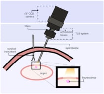
Volpi and colleagues have developed a tunable lens systems (TLS), a device that exploits electronics to change focus during operation, that can be integrated into commercially available laparoscopes (Biomed. Opt. Express8 3232). While common in consumer cameras, such adjustable focus control has not yet been incorporated into a clinically viable setup. Furthermore, the research team made their device suitable for fluorescence-guided surgeries, for which it is vital to keep the light free of distortion as it passes through the lens.
The optical performance of the Oxford team’s TLS offers two key advantages. First, its fast response time of less than 7.5 ms allows it to switch focus extremely quickly, potentially allowing a fully autofocus capability or the use of two or three preset focus points (see visualization below).
Second, the TLS has been specifically designed to prevent the light distortion caused by chromatic aberrations. This is important for fluorescence-guided surgeries, since the most effective biomarkers generate fluorescence in the near-infrared (NIR). Optical tests showed that the TLS offered achromatic performance in the visible and NIR, enabling simultaneous imaging of white-light reflectance and fluorescence from the biomarkers.
Volpi and collaborators show in their paper also tested the performance of the TLS on animal models, obtaining in vivo images of tumours in mice. Fluorescence images obtained with a laparoscope fitted with the TLS appear noticeably sharper than a similar system equipped with a visible-NIR lens, suggesting that the TLS offers a viable option for fluorescence-guided laparoscopy surgeries in the clinic.
Macrophages – the ‘big eaters’ within the immune system – could offer new insights into cell migration if it were possible to accurately visualize their interactions. But researchers still struggle to distinguish overlapping cells in microscope images, which makes it difficult to locate and track these cells. While various methods have been used to segment overlapping cells, a UK team of biomedical engineers, computer scientists and biologists have now worked together to develop an automatic algorithm that could improve these techniques, and also enable more accurate cell location and tracking (MIUA 2017).
The accurate segmentation of biomedical images is a key focus for researchers who are trying to improve image analysis of overlapping cells. José Alonso Solís-Lemus and co-workers at City University of London and King’s College London have now developed an algorithm that improves the detection and segmentation of fluoresced overlapping cells of fruit fly embryos (Drosophila melanogaster). The algorithm, called Anglegram, offers new insights into how macrophages use signals to help them migrate.
Anglegram reveals junctions between overlapping cells
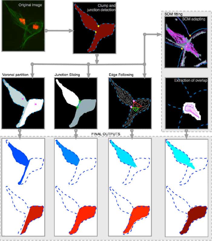
In the fluorescence images analysed by the team, the red signal corresponds to the cell nuclei, while the green represents the intracellular proteins, known as microtubules. The key challenge when analysing these images is that the green fluorescence from the microtubules are not strong enough to accurately determine the cell segmentation.
Anglegram combined with junction splicing provides the most accurate cell segmentation
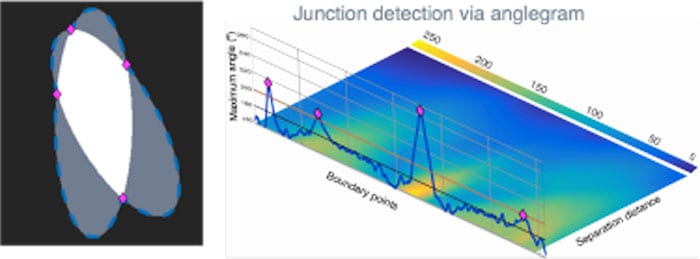
The Anglegram algorithm can help when a cluster of two or more overlapped macrophages is detected by the presence of two or more red nuclei. The algorithm works by automatically detecting the junctions between overlapping cells, as determined by the inner angles of the cell boundaries. This produces a 2D matrix resembling a heat map, which is known as the Anglegram. Boundary points representing the junctions can then be located based on the maximum intensity projection of the Anglegram matrix.
The researchers tested the performance of the Anglegram algorithm by combining it with three different segmentation methods, and comparing the results with a fourth technique that was used on its own as a benchmark. All segmentation methods differ in the way they operate, but the junction slicing technique produced the most accurate segmentation when combined with Anglegram.
The results suggest that Anglegram offers a promising method for improving the segmentation of overlapping cells. Further development of the algorithm could eventually make it possible to detect overlapping cells when more than two cells are clumped together.
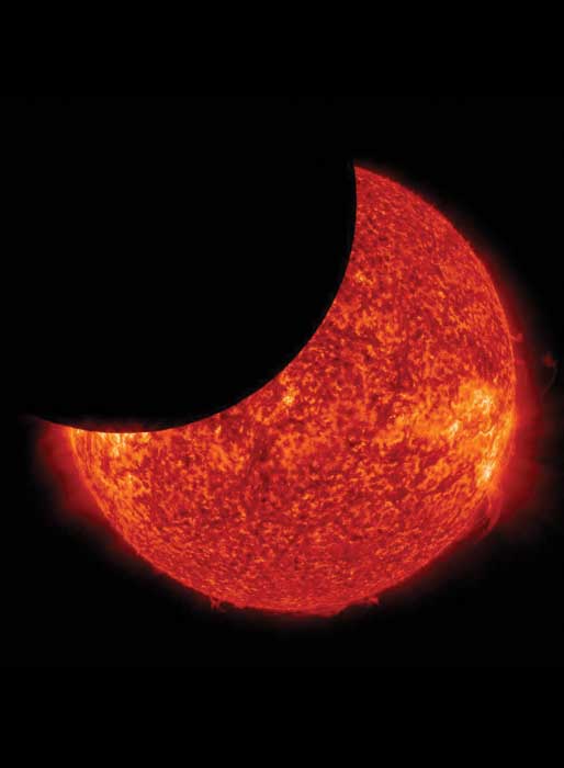
It’s safe to say that finding a book about eclipses is an easy task – they number in the hundreds and vary from tiny pocketbooks to glossy coffee-table books with incredible pictures. In this saturated market, it can be difficult to pick out a useful guide to learning about eclipses and how to view them. In case you are lucky enough to be in the path of the upcoming eclipse this month, but don’t feel fully prepared when it comes to, say, photographing this seemingly rare event, or you are really keen on getting to grips with the science in detail, then Totality: the Great American Eclipses of 2017 and 2024, written by Mark Littmann and Fred Espenak, is the book for you.
At first glance, it may come off looking too much like a science textbook, and in some ways it is. But don’t let that put you off. Littmann is an award-winning astronomy writer, while Espenak is better known as “Mr Eclipse” and between the two of them, Totality covers pretty much everything you would possibly want or need to know about eclipses. The book is detailed, but the language is clear, simple and even poetic at times, as the authors describe each aspect of an eclipse.
The chapters cover everything from the mythology and lore of eclipses; how our understanding of these events has grown over the millennia; the scientific impact of eclipses, including the eclipse of 1919, which the authors describe as the “eclipse that made Einstein famous”; and of course step-by-step guides on how to safely observe and photograph a total solar eclipse. The chapter on photography is especially useful for those who may be keen on capturing this event but are unsure of what works and what equipment is necessary. Littmann and Espenak explain how even the simplest of cameras or a smartphone can be used, while also detailing techniques for those with more photographic equipment and/or ability. Each chapter is full of tables, charts, diagrams and maps, so if an in-depth study on all things eclipse-related is what you are looking for, then get a copy of Totality.
On 30 September 1131 BC, according to physicist and science writer Frank Close, the prophet Joshua looked to the heavens and witnessed one of several solar eclipses mentioned in the Old Testament. But what makes this event special for Close is Joshua’s description of the Sun stopping in the sky and the Moon reversing direction during the eclipse. As a scientist, Close knows that the Moon does not go into reverse, so he was convinced that Joshua experienced an optical illusion – and he wanted to see it too. Eclipse: Journey to the Dark Side of the Moon is the story of Close’s obsession with solar eclipses, which began 63 years ago in East Anglia, UK, where an eight-year-old Close experienced a partial eclipse. Since then, he has travelled to the ends of the Earth to witness total eclipses – racing across the sands of Libya and chasing the darkening Sun on both the Pacific and Atlantic Oceans. Indeed, it was while bobbing off the coast of Fiji in less-than-perfect weather conditions that Close finally experienced the “Joshua illusion”. Much of the book is travelogue, and provides a taste of the package tours that take enthusiasts to some of the most improbable places in search of totality. Close also includes a few amusing anecdotes about his fellow fanatics – including one man who seemed convinced that he was going to be plucked off a boat by an alien spacecraft during an eclipse. Close stresses that every eclipse is unique, with an event in the desert being very different from one witnessed at sea. The hook for this book is the total eclipse that will sweep across a vast arc of the US on 21 August. Close wraps up his book with a few tips on how to best view the event – avoiding clouds and traffic jams when possible. And if you miss this month’s eclipse but happen to be in North America in 2024, an eclipse will sweep across Mexico, the US and Canada.
Precious elements may come from spinning neutron stars that have swallowed a tiny black hole and imploded. If true, this dramatically changes our understanding not only of how rare elements like gold are made, but also the nature of some dark matter.
The elements in question include all atoms heavier than bismuth, as well as some neutron-rich isotopes heavier than iron. They are forged in what is called the r-process (meaning ‘rapid’), which requires copious numbers of neutrons as well as densities ten billion times greater than those found in the Sun’s core to enable the rapid capture of those neutrons by atomic nuclei. Therefore, the r‑process can only take place in the most extreme environments.
In 1957, Burbidge–Burbidge–Fowler–Hoyle (known as B2FH) proposed that core-collapse supernovae were the origin of the r‑process elements, but in recent years this has fallen into doubt. Binary neutron star mergers have emerged as a frontrunner, but there’s a problem: with an estimated merger rate of one per 100 000 years, computer simulations struggle to recreate enough r-process elements.
If George Fuller of the University of California, San Diego and his colleagues Alex Kusenko and Volodymyr Takhistov of the University of California, Los Angeles are right, then it’s time for a new explanation. They propose that tiny primordial black holes could become lodged inside a neutron star’s core, where the black hole begins to consume matter and grow. As the neutron star’s interior swirls around the black hole that is eating it, the neutron star begins spinning rapidly and ejects up to a tenth of a solar mass of neutron-rich material into space. This dense material decompresses, allowing beta decay to transform some of the neutrons into protons, which is followed by the rapid formation of massive atomic nuclei.
Hypothetical black holes
The hypothesis, presented in Physical Review Letters, hinges on the requirement that “a few per cent or more of the dark matter is comprised of black holes,” Fuller says. Conceived by Stephen Hawking and theorized to have formed in the immediate moments after the Big Bang, researchers are yet to discover a primordial black hole, which would have a mass similar to that of an asteroid. If they do exist, they would follow the distribution of dark matter, with many of them in the galactic centre. Much like dark matter, they would barely interact with ordinary stars and planets. It’s only neutron stars that would be dense enough to capture them.
Nor should we worry about one hitting Earth. “In the entire history of our planet there is a chance of between 1 in 10 000 and 1 in 100 000 that one of these primordial black holes would pass through Earth,” explains Fuller. “It would just go right through and certainly wouldn’t be stopped by the Earth.”
Things now hinge on observations. Merging neutron stars produce gravitational waves as they spiral into a collision. The Advanced LIGO gravitational wave detector should be able to detect these final stages of a merger at a rate of at least 40 per year, out to a distance of 650 million light years.
“That’s the supreme court in my view,” says Fuller. “If we see binary neutron star mergers with LIGO, then we’ll get a thumbs-up or a thumbs-down on whether the merger rate is high enough.”
Smoking gun
Meanwhile, we may already have found evidence for neutron star–primordial black hole interactions without realizing it. Mysterious fast radio bursts (FRBs) could originate from the neutron star implosions. The destruction of neutron stars could also explain why there are fewer pulsars found in the galactic centre than expected, while beta decay during the r-process could provide the anomalous positron signal at 511 keV that comes from the centre of the Milky Way.
More direct evidence for neutron star implosions could come in the form of kilonovae – bursts of light with a tenth to a hundredth of the brightness of a normal supernova and which are currently thought to be the “smoking gun for a binary neutron star merger and r-process production”, says Fuller. However, if we detect a kilonova within 650 million light years without any accompanying gravitational waves, “that would be suspicious and would look a little bit like the destruction of a neutron star, either by our black hole scenario or by eating some other kind of dark matter and being destabilized”.
There could still be a bump in the road. Earlier this year, Tim Linden of Ohio State University and Joseph Bramante of the Perimeter Institute published a pre-print on arXiv suggesting that low-mass dark matter particles could also accumulate within neutron stars, causing them to implode.
Linden says that he and Bramante calculated the interaction rate between neutron stars and primordial black holes as being “significantly smaller” than that calculated by Fuller’s team. “This is primarily due to different assumptions for the velocity dispersion of neutron stars and primordial black holes very near the galactic centre,” Linden explains. The two groups plan to sit down in the coming months and address these differences.
In the late summer of 1864, anyone wanting to travel along the east side of Crystal Palace Park in London could buy a train ticket for sixpence – but this was no ordinary railway. Designed by the British engineer Thomas Webster Rammell, the Crystal Palace pneumatic railway consisted of a carriage that fitted snugly inside a tunnel, such that when a huge fan was turned on, the carriage was sucked from one end of the tunnel to the other. Average speeds of around 40 km/h meant that passengers could make the 550 metre trip in a little under a minute – twice as fast as the carriage’s horse-drawn competitors.
Rammell’s pneumatic railway was experimental, and it only ran for two months. A century and a half later, however, the idea of getting from A to B inside depressurized passages is back, thanks to another entrepreneurial visionary: Elon Musk, the South-African born, Canadian-American multibillionaire behind Tesla electric cars and SpaceX rockets. In 2013 Musk published a white paper outlining the concept of a hyperloop: an evacuated steel tube through which passenger “pods” travel cheaply and efficiently over continental distances. Thanks to the minimal air resistance, Musk claimed, the pods could be accelerated to speeds of up to 760 km/h.
The hyperloop sounds almost too good to be true, and many critics have said as much, branding Musk’s idea impractical, unsafe and – for various political and economic reasons – unrealizable. But in the four years since Musk’s white paper, at least three major start-ups have been created, and dozens of academics and industry professionals have climbed on board – figuratively if not yet literally. Their hope is to revolutionize public transport and, in so doing, restructure society for the better.
Simple on paper
Few deny the basic principles behind the hyperloop. At atmospheric pressure, air resistance mounts swiftly with speed, which is why supersonic jets tend to fly at high altitude. To avoid consuming huge amounts of energy, therefore, a near-sonic or supersonic vehicle at ground level needs an evacuated environment in which to travel. A tube is the obvious solution, although one containing a near vacuum would have to be resistant to the tiniest crack or leaky seal. For that reason, Musk proposed a tube containing merely low-pressure air, at about one millibar.
This residual air brings a problem, however, in that a snugly-fitting vehicle will, at high speeds, have to push an entire air column ahead of it – “not good”, in Musk’s words. The entrepreneur therefore proposed mounting a compressor fan in the nose of the hyperloop pod to transfer air backwards. In fact, he said, the air could even be channelled beneath the pod, creating a cushion for the pod to ride on, like an air-hockey puck. Meanwhile, contactless linear induction motors, placed at intervals along the tube, would supply an alternating magnetic field to accelerate the pod.
Musk claimed that he and his SpaceX company were too busy to work on a hyperloop themselves (other projects in the works include a plan to colonize Mars), but he encouraged others to pick up the baton. Within months a German entrepreneur, Dirk Ahlborn, obliged by setting up Hyperloop Transportation Technologies (HTT) in the US; hot on his heels came Shervin Pishevar, an Iranian-American entrepreneur who was reportedly responsible for persuading Musk to release the hyperloop white paper in the first place. Pishevar called his US company Hyperloop Technologies, though it was subsequently rebranded as Hyperloop One.
Both HTT and Hyperloop One claim to have amassed investments of $100m or more. Both, too, have revised various aspects of Musk’s original design, favouring different implementations of magnetic levitation, or “maglev”, over air cushioning. But concrete advances have been slower. HTT has gone quiet on previous claims that it would have a prototype hyperloop running as soon as 2018. Hyperloop One has delivered more visible progress, carrying out a linear-motor propulsion test just north of Las Vegas, US, in May 2016; on the other hand, its “first flight” of a fully functioning hyperloop, scheduled for early 2017, had not yet taken place at press time.
A third start-up, TransPod, entered the scene in 2015. Although this Canada-based firm has had less public exposure than HTT and Hyperloop One, co-founder Ryan Janzen believes it stands a better chance of success because none of its major components are going to come off the shelf; instead they are all being designed specifically to suit the needs of their hyperloop technology, drawing on expertise from across the rail, aerospace and space, and architecture sectors. “I like to say that we’re building a spacecraft that’s shaped like a plane, and operates like a train,” Janzen says.
TransPod hopes to deliver a “commercially viable product” by 2020, and has developed algorithms that can design optimal routes between cities, taking into account geography and existing infrastructure. One of the routes it is considering is the 550 km stretch between Toronto and Montreal, which currently takes one and a half hours by plane or up to six hours by car. A hyperloop, TransPod claims, could cut this journey time to 45 minutes.
Path to success? Hyperloop One’s “DevLoop” test track in Nevada, US, nears completion. (Courtesy: Hyperloop One)
Like many hyperloop proponents, Janzen believes the infrastructure cost would be roughly similar to that posed by high-speed rail, which is seen as the main competitor. But many independent engineers are sceptical about this, given the cost overruns that often occur with major infrastructure projects, even when the technologies involved are well-established. (In the UK, for example, cost estimates for a proposed north-to-south high-speed railway have spiralled from £30bn to more than £80bn.) And as control-systems engineer Roger Goodall at Loughborough University in the UK explains, cost is not the only potential barrier. Among his concerns are the integrity of evacuated tubes over large distances, especially when tubes have to fork into different routes, and the possibility that passengers would have to stomach accelerations of 0.5 g on banked curves. “I suspect that working, eating and certainly moving around during the journey would not be a possibility,” he says. “Overall, it seems an interesting thought exercise for STEM students, [but] I am astonished by the substantial developments going on in the US.”
Others, though, have been less quick to dismiss the idea. Carl Brockmeyer, head of business development at the Germany-based vacuum technology company Leybold, read about hyperloops after they were first proposed and immediately wanted to get involved. “We’re not the type of people who say, ‘You’re crazy’,” he explains. “We’re the type of people who say, ‘Cool, how can we help?’” Leybold is now working with both Hyperloop One and HTT.
Brockmeyer isn’t fazed by the scale of the vacuum system required. He points out that Leybold helped to deliver the 27 km long vacuum system at the Large Hadron Collider at CERN on the Franco–Swiss border; that system needed pressures in the region of 10–11 millibar, some 11 orders of magnitude less than a hyperloop would require. “I don’t want to say ‘simple’, but let’s say it’s very achievable,” Brockmeyer says, referring to hyperloop’s pressure requirements. “We’ve delivered vacuum systems that are technically far more challenging.”
Old news?
Indeed, perhaps the hyperloop is not as cutting-edge as it appears. In the early 1980s researchers at the Swiss Federal Institute of Technology in Lausanne (EPFL) began investigating the possibility of creating an underground network of tunnels to connect the major cities of Switzerland. Known as Swissmetro, the system would have employed maglev trains travelling through reduced air pressures at speeds of up to 450 km/h.
The initial reception for Swissmetro was positive: a preliminary study was supported by the federal government, a more substantial analysis backed by the state and private sector followed, and by the late 1990s there were grounds for industrial development. But within a few years the government’s interest had waned amid claims that the system was not economically viable. Marcel Jufer, the engineer who led the EPFL group, believes the reason was that the government had already committed to building the Gotthard Base Tunnel, which runs under the Alps between Erstfeld and Bodio and is now, at 57 km, the world’s longest railway tunnel. After Swiss voters approved this north–south tunnel in 1992, there was simply no money left for an east–west Swissmetro, which Jufer says would have cost about the same. Whatever the real reason, in 2009 the Swissmetro company went into liquidation, although the EPFL group went on to discuss similar projects in South Korea and Belgium.
Should Swissmetro be taken as a salutary lesson for eager proponents of hyperloops? Jufer does not think that the new start-ups will necessarily suffer the same fate, but he knows not to underestimate the politico-economic challenges. HTT has bragged that landowners will welcome elevated hyperloop tubes running across their property in return for in-kind benefits such as free electricity, but Jufer believes the tubes would be better off buried underground to avoid any possibility of nimbyism. Though that might sound like a more expensive option, John Miles, an engineer at the University of Cambridge in the UK, points out that hyperloop tunnels would only need to be a fraction of the diameter of railway tunnels and so costs would be dramatically less.
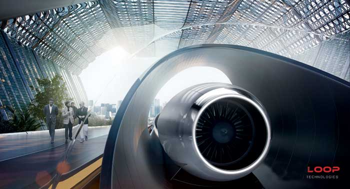
The future has arrived An artist’s impression of what a hyperloop station will look like. (Courtesy: Hyperloop Transportation Technologies)
Jufer also stresses the influence of vested interests, in the form of existing rail companies. Contrary to the vision of, for example, Hyperloop One, which is exploring routes between major European cities – partly, it seems, as a marketing exercise – Jufer believes a better place to start would be somewhere like Brazil, which does not already have strong rail infrastructure. “It takes a long, long time to overcome political problems,” he says.
Obstacles to overcome
Hyperloops have no shortage of other criticisms. Sceptics have claimed that the systems will be highly susceptible to everything from power outages and acoustic noise to earthquakes and terror attacks. Although some hyperloop proponents have compared the technology to airplane travel, “a plane does not travel at 1000 km/h a few centimetres from a steel wall,” observes Paolo Chiggiato, who leads the vacuum, surfaces and coatings group at CERN. “In case of a lack of electrical power, the vessel would inevitably touch the walls or the rails on which it is normally suspended. If a shock provoked a failure in the vessel tightness, the passengers would be rapidly surrounded in vacuum.” A pressure of 1 mbar, he notes, is equivalent to atmospheric pressure 50 km above the Earth’s surface – more than 10 times higher than the cruising altitude of a typical jetliner.
There has been backroom controversy, too: last year, Hyperloop One had to settle a lawsuit filed by one of its co-founders and three other employees alleging corporate malpractice. And within the academic community the debate has not always been constructive, as rail engineer John Preston at the University of Southampton in the UK found when he attended a transportation conference in South Korea in June 2017. “There was an interesting clash between the mainstream maglev supporters and the hyperloop ‘interlopers’ on comfort and cost, but with little clarity on either except for a diversion on virtual windows,” he says.
Despite these critiques, though, some experts think it is lazy to dismiss hyperloops out of hand based on the futuristic appearance of the technology. “The natural inclination of everyone is to say it’ll never happen,” says Miles. “And before you get excited about anything you should always do some calculations. But having done those, I found that I became more inclined to believe it could happen, rather than less inclined.” Miles persuaded his former employers, the international consultancy Arup, to begin offering expertise to Hyperloop One on a non-contractual basis.
Miles is well aware of the potential technological problems. “If you put high voltage inside a vacuum tube, you end up with what is effectively a strip light,” he jokes, by way of example. But he points out that each of hyperloop’s key components – propulsion, levitation, guidance, control and reduced pressure – are all technologies that have been well established in different spheres. The goal now is to get them to work in concert.
The new Tube
The Victorians would not have been daunted by such a challenge. While passers-by marvelled at Rammell’s pneumatic railway, engineers elsewhere in London were toying with the dubious idea of an extensive underground railway, at a time when most of the city’s inhabitants were still travelling by horse and cart. “The ability to effectively introduce the London Underground at the national scale, if you could do it, would quite simply transform the economic outlook for the UK,” says Miles. “Yes, it’s quite a challenge. But having spent a fair bit of time on this now, I’ve yet to see anything that I’d regard as a showstopper.”