Jumping droplets could cool computer chips

When two droplets coalesce on some water-repellent materials, the resulting droplet will jump away from the surface – a process that removes dirt from some biological surfaces such as cicada wings. Now, researchers at Duke University in the US have harnessed this curious effect to create a technique for drawing heat away from “mobile hotspots” on the surfaces of microelectronic devices. The method could therefore be a new way for cooling microprocessor chips, which are becoming increasingly hard to cool as they become smaller and operate at ever higher frequencies.

The system developed by Duke’s Chuan-Hua Chen and colleagues consists of a sealed, disc-shaped chamber that is about 2 mm thick and contains water vapour. One inside surface of the chamber is made from a superhydrophilic (highly water-retaining) material covered with a water-absorbing wick. The opposite surface is superhydrophobic (highly water-repelling), on which water forms mobile droplets.

Condensing droplets

The superhydrophilic side is placed next to the surface to be cooled (see figure and video), which causes heat from a hot spot to be transferred to it. Water on the heated superhydrophilic surface therefore evaporates into the chamber, cooling the surface and hot spot. Most of this vapour travels across the 2 mm gap and condenses on the opposite superhydrophobic surface, where it forms droplets.

These droplets then rapidly coalesce, jump away from the surface and end up right back at the hot spot on the opposite superhydrophilic surface. The jumping droplets therefore replenish the supply of cooling water to the hot spot. If the hot spot moves, the evaporation-jumping cycle will simply occur at the new location.

Mobile hot spots occur in different places on a chip at different times, depending on what tasks the chip is performing. It can be difficult to predict where and when these hot spots will occur, and this transient nature makes mobile hot spots difficult to deal with using simple, low-cost passive cooling. Instead, more complicated and costly active cooling systems must be used. Chen’s team believes its device could solve this problem.

Comparable to copper

While the Duke technique demonstrates the principle of using jumping drops for cooling, the team now needs to find suitable surface materials that will function for long times when subjected to a high-temperature vapour. “It has taken us a few years to work the system to a point where it’s at least comparable to a copper heat spreader, the most popular cooling solution,” says Chen. “But now, for the first time, I see a pathway to beating the industry standard.”

The new cooling device is described in Applied Physics Letters.

The STAR of the show

By Michael Banks

You may remember in 2014 when we reported that entrepreneur Richard Dinan – a former star of the UK reality-TV programme Made in Chelsea – was venturing into fusion energy.

He founded the firm Applied Fusion Systems with the aim of building a prototype fusion reactor. The 30 year old, who doesn’t have a university degree, claims to have taught himself tokamak design and employs a small team of scientists who are working on a design.

Well, the firm has now released its first blueprint for a spherical fusion tokamak and is seeking £200m in investment to build not one, but two of the machines.

(more…)

Flash Physics: Antineutrino anomaly not sterile neutrinos, laser boosts protons, silicon-III is a semiconductor

Antineutrino anomaly is a calculation error, not sterile neutrinos

An error in how antineutrino production is calculated could be responsible for the mismatch between measurements of the numbers of antineutrinos produced in nuclear reactors and theoretical predictions. That is the conclusion of an international team of physicists working on the Daya Bay Neutrino Experiment at a nuclear-power complex in China. Nuclear fission in commercial reactors creates huge numbers of antineutrinos, which can then be detected by the Daya Bay experiment and other detectors located near to reactors worldwide. Since 2011, physicists have noticed that significantly fewer antineutrinos are detected by these experiments than predicted by theory. Some have speculated that the missing particles had morphed into sterile neutrinos on the short journey from reactor core to detector. Sterile neutrinos are hypothetical particles that could account for some of the mysterious dark matter that is thought to pervade the universe – and therefore any evidence of sterile neutrinos is of great interest to physicists. The Daya Bay team has looked at the antineutrino flux from two main fission isotopes in the reactor core – uranium-235 and plutonium-239. The researchers were able to show that the measured flux from plutonium-239 matches theoretical predictions – which suggests that antineutrinos from this isotope are not morphing into sterile neutrinos. As a result, they conclude that the current theory incorrectly predicts an over-production of antineutrinos by uranium-235 fission of about 8%. Writing in a preprint on the arXiv server, they point out that their conclusion could be tested by future experiments based at reactors fuelled with high-enriched uranium.

Proton beam boosted by combining laser bursts

Proton beams have been produced by using a prolonged laser burst of lower than expected energy. Proton-beam systems are receiving increasing attention because of their application in cancer treatment. One method for producing the beam of charged particles is laser-plasma acceleration. This is when powerful lasers are fired at ultra-thin metal foils, producing a plasma in which electrons separate from ions. The resulting huge electric fields can accelerate protons, ions and electrons to high energies. Typically this is done with a burst of high-contrast laser light, a single picosecond in length. While polarized light and repeated pulses have shown promise in improving the quality of proton beams, little is known about using longer bursts of light because such intensely powerful lasers can only be generated for a short time. Now, scientists at Osaka University have used one of the world’s most powerful lasers, the Laser for Fast Ignition Experiments (LFEX), to study longer bursts. “By carefully timing the firing of four beams, it was possible for us to effectively fire each in sequence to generate longer pulses that otherwise had the same sharp features as single pulses,” says group leader Hiroshi Azechi . The configuration meant that the laser light could be 100 times less intense than previously thought necessary to produce high-energy protons. “Using multiple pulses to create a longer pulse heats up the electron plasma significantly, which is likely what causes the charged particles to achieve a higher energy at a lower laser intensity,” explains team member Akifumi Yogo. The finding, presented in Scientific Reports, could lead to more efficient proton beams and provide increased precision for medical applications. For more on proton therapy for cancer treatment, see the free Physics World Discovery ebook Proton Beam Therapy.

Silicon-III is a semiconductor, not a metal

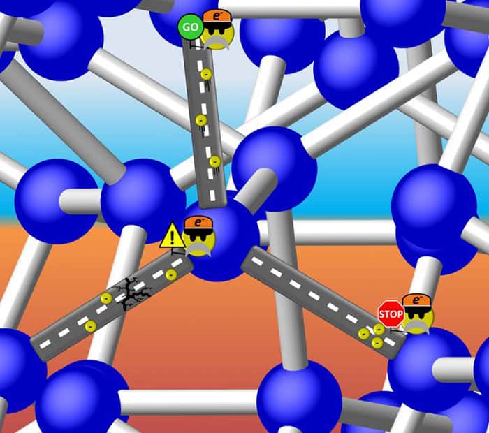
Illustration of electrons in silicon-III

Silicon normally adopts a diamond-like crystal structure, but under the right conditions it can assume several other structures including silicon-III, which has a cubic structure with 16 atoms in a unit cell. Previous studies had suggested that silicon-III is a poorly conducting metal without an electronic band gap. But now physicists in the US and France, led by Tim Strobel at the Carnegie Institution for Science in Washington DC, have made and studied pure bulk samples of silicon-III and shown that the material is actually a semiconductor with a very narrow band gap. They made their samples by applying extreme pressure to normal silicon and confirmed that they were pure silicon-III using X-ray diffraction, Raman spectroscopy and nuclear magnetic resonance spectroscopy. They then did a series of experiments on the samples that looked at the optical, electrical and thermal properties of the material. Together, these measurements show that silicon-III has a band gap of about 30 meV, which is much smaller than the 1.1 eV band gap of conventional silicon. Unlike conventional silicon, silicon-III has a direct band gap. This means that electronic transitions in the material can involve the direct emission of a photon. The band-gap energy of 30 meV corresponds to an infrared photon, so silicon-III could be particularly useful in future plasmonic devices that could operate at that energy. The work is described in Physical Review Letters.


  • You can find all our daily Flash Physics posts in the website’s news section, as well as on Twitter and Facebook using #FlashPhysics.

Miniature X-ray detector uses nano-antenna

Scientists in France have developed a tiny X-ray detector at the tip of an optical fibre. By combining a nano-optical antenna (NOA) with indirect detection methods, the team has created a device that is only a few tens of microns in diameter. It could therefore have applications in medical endoscopy dosimetry.

Many of today’s X-ray detectors rely upon indirect measurements, whereby a scintillator first converts X-ray energy into light. The photons then travel through optical fibres to a camera or photodetector. While this set-up is widely used in medicine and industry, the machines are cumbersome and creating a small-scale version is challenging. The quantity of X-rays detected is dependent upon the size of the scintillator and the resulting photons are emitted in all directions. Therefore, a small scintillator produces very few photons and the likelihood of them emitting in the direction of the camera is low.

To overcome this problem, Thierry Grosjean, from the University of Burgundy–Franche-Comté in France, and colleagues, incorporated a nano-optical antenna (NOA) between a small scintillator cluster and an optical fibre. Analogous to a microwave horn antenna, a NOA can direct light. So, when an X-ray hits the tiny scintillator cluster, the light emitted can be directed down a thin optical fibre to the camera, thereby increasing the amount of photons detected.

Tiny antenna

The NOA is a miniature horn antenna – it contains a flared wave guide that amplifies a dipolar signal and directs it into a linear waveguide. To create the device, the team grew a 38 μm-long polymer microtip (tip radius 1 μm) at the end of a thin optical fibre. The scintillation cluster was then grafted onto the tip. To prevent visible light from entering the system, a thin layer of aluminium and titanium was applied to its surface. “Such a cluster-to-fibre coupling enhancement enables the realization of X-ray detectors at the end of a narrow single-mode fibre – 125 μm outer diameter in our study, or less,” explains Grosjean.

As well as miniaturizing X-ray detection, a key challenge was to design a device that could be made at low-cost and has the potential to be mass-produced. The researchers point out that the resulting detectors are inexpensive to make and do not require clean-room processes to be fabricated.

The researchers have tested their device for soft X-rays (low energy radiation around 10 keV). They have achieved a spatial resolution in the order of 1 μm, although they hope to improve this to 100 nm in future work to distinguish chemical components during low-energy X-ray scanning microscopy.

Endoscopic dosimeter

“The next step will be to demonstrate our concept with high-energy X-rays for medical applications,” says Grosjean. The compact nature of the device means it could be incorporated into endoscopy techniques and used to measure radiation exposure from inside the body during radiotherapy cancer treatment. To proceed with the work, the group has applied for funding from the French National Research Agency and hopes to produce a market-ready prototype within three years.

“The compactness of our sensor is unprecedented,” Grosjean concludes, “Our nano-optically driven technology is totally new.” The work is presented in The Optical Society journal Optics Letters.

Flash Physics: Memristors are good synapses, graphene-oxide desalination, surface tension higher for short times

Why memristors make good artificial synapses

An international team of researchers has worked out why a ferroelectric memristor does a good job at mimicking an important function of the brain. The brain learns by reconfiguring the strengths of the connections (synapses) between neurons and in a process that is called synaptic plasticity – and researchers are keen on creating artificial brains that learn in a similar way. Vincent Garcia and colleagues at CNRS, Thales, and several universities in France, the US and Switzerland have studied synapses that are based on ferroelectric tunnel junctions (FTJs) that adhere to a biological learning rule called spike-timing-dependent plasticity (STDP). Each FTJ measures less than one micron across and comprises a thin ferroelectric layer sandwiched between two electrodes. The FTJs operate as memristors, whereby the resistance of the layer can be tuned using voltage pulses similar to those in neurons. If the resistance is low the synaptic connection will be strong, and if the resistance is high the connection will be weak. This capacity to adapt its resistance enables the synapse to learn. While FTPs are used as artificial synapses in many laboratories, exactly how they function was not well understood. Now, Garcia and colleagues claim to be the first to have developed a physical model that describes how the artificial synapses work. Using a combination of experimental measurements they have shown that changes in the resistance of the FTJs are brought about by the nucleation-dominated reversal of ferromagnetic domains. Writing in Nature Communications, the team says it was able to simulate the behaviour of an artificial neural network based on an array of FTJs and show that it should be capable of learning to recognise patterns. Garcia and colleagues now plan to use the FTPs to develop a camera that can perform real-time shape recognition. There is more about artificial neural networks in “Smarter machines” (subscription required).

Graphene oxide turns seawater to drinking water

Artist's impression of graphene oxide membrane removing salt from seawater

Graphene-oxide sieves have turned seawater into drinking water. Over the past five years, a team at the University of Manchester in the UK has studied using graphene and graphene oxide as a way of removing salt from seawater, with the aim to replace current, energy-intensive methods. While plain graphene is just a single layer of carbon atoms, graphene oxide (GO) is covered with molecules such as hydroxyl groups. As graphene is impermeable to gases and liquids, holes have to be drilled through to create a sieve. “But if the hole size is larger than one nanometre, the salts go through the hole,” explains team member Rahul Nair, “You have to make a membrane with a very uniform less-than-one-nanometre hole size to make it useful for desalination. It is a really challenging job.” In contrast, GO is permeable and easier to make. Nair and colleagues have previously found that GO can remove small nanoparticles, organic molecules and large salts, however, as with graphene, common salt (sodium chloride) has proven more difficult because it is smaller. Now, the researchers have demonstrated that walls of epoxy resin on either side of the GO membrane prevent it’s natural expansion in water, and this has allowed them to create a sieve with only 7.8 Å spacing, rather than 9.8 Å. These tiny pores through the membrane mean that water molecules can still penetrate but salt cannot. The group hopes the current work, presented in Nature Nanotechnology, may lead to a cheap and efficient method for producing clean drinking water from seawater.

Surface tension of water can be much greater than previously thought

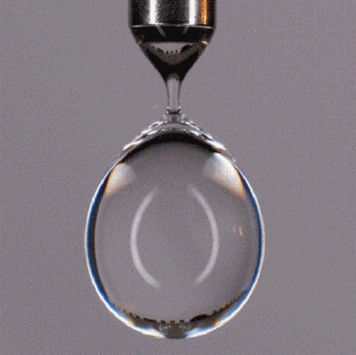
High-speed camera image of a water droplet

The surface tension of water can be much higher than the currently accepted value. That is the surprising conclusion of Ines Hauner and Daniel Bonn of the University of Amsterdam and colleagues in the Netherlands, France and Australia, who measured the surface tension of newly created water–air interfaces. They found that at times up to about 1 ms after the new interface is created, the surface tension of the water can be as much as 25% greater than the accepted room-temperature value of 72.75 mN/m. This could have important implications for industrial processes such as inkjet printing, which rely on the rapid formation of tiny droplets – a process that is governed by surface tension. The team made its discovery using a high-speed camera to watch the release of water droplets from a tap. This involves the formation of a liquid neck on which the drops hangs before breaking away – and by analysing this process on a sub-millisecond timescale, the researchers were able to calculate the surface tension. The study is described in The Journal of Physical Chemistry Letters.


  • You can find all our daily Flash Physics posts in the website’s news section, as well as on Twitter and Facebook using #FlashPhysics.

Doughnut-shaped nanomagnets induce new magnetization states

Magnonics (the study of excitations in a magnetic material) may well replace electronics as the basis of modern computing. This would drastically increase energy efficiency and provide devices that can be miniaturized beyond the limit of current technology. However, the control of magnetic textures in nano-sized magnets is not straightforward to achieve. A team of researchers in Brazil and Chile have found a novel and elegant way to create stable magnetic configurations that had previously not been possible.

The direction of magnetization within a ferromagnetic material may take on many exotic configurations. For example, a vortex forms when the magnetization spirals inward towards a single point. Such magnetic textures appear in domain walls and as ground-state configurations in some sub-micron-sized magnetic elements.

An antivortex is formed when the magnetization spirals outwards from a single point and has an opposite winding number to a vortex. The ability to manipulate magnetization vortex–antivortex pairs opens up a number of potential applications in computing and data storage. However, while stable vortices have been observed in various systems, a stable antivortex had proved difficult to obtain. Now, Smiljan Vojkovic and colleagues at Pontificia Universidad Católica de ChileUniversidad de Chile in Chile, and Instituto Federal de Educação, Ciência e Tecnologia Baiano and Universidade Federal de Viçosa in Brazil have cracked it by incorporating curvature into their nanomagnets.

The twist with donuts

Inducing a strong curvature in a magnetic material breaks the inversion symmetry, giving rise to a twist in the magnetization, with the direction of the twist depending on whether the curve is positive like a sphere or negative like a hyperboloid. The research team designed and modelled a nanomagnet in the shape of a hollow doughnut-shape, or torus, which has negative curvature on the internal border and positive on the external border. They exposed this to an external magnetizing field in the plane of the torus and monitored the remnant magnetization left behind after this field was removed. Indeed, at each of these borders a stable vortex or antivortex was formed according to the direction of the curvature.

The next challenge for the researchers is to manipulate these vortex–antivortex pairs. If it is possible to transfer the pair to a straight wire without damage, magnetization-based logic operations may become possible. “Race-track” memory devices could be designed around these magnetic configurations, which would allow data storage density to exceed the fundamental limit of current devices. Furthermore, the use of an oscillating external field would lend these structures to the design of nanoscale antennas.

More details can be found in the original article in the Journal of Applied Physics.

Microfluidic chip can detect HIV and MRSA

A team of biophysicists and bioengineers in the US have developed a $10, self-powered microfluidic chip that can rapidly detect disease-related RNA or DNA in blood samples. The chip is faster and significantly cheaper than current lab-based detection methods. The researchers say that it could be particularly useful in low-income parts of the world and could open the door to affordable preventative healthcare for everyone.

There is a lot of interest in developing low-cost, portable nucleic acid (RNA and DNA) detection technologies, which could diagnose important diseases and revolutionize preventative medicine. Current standard methods for amplifying and detecting nucleic acids are based on a method known as polymerase chain reaction (PCR). This is an expensive technique that requires trained technicians, multiple sample preparation steps, and powered laboratory equipment such as centrifuges, making it impractical in low-resource settings, small clinics and at home.

Simple point-of-care tests for diseases are available, but these detect protein biomarkers and lack sensitivity. This means that patients are often unwell before they are tested, reducing the possibilities for preventative treatment. “It is time to use sensitive and quantitative circulating nucleic acids-based molecular diagnostics,” explains Luke Lee, a biophysicist and bioengineer at the University of California, Berkeley. “[These techniques] can identify diseases early, instead of just confirming them.”

Vacuum battery

Writing in Scientific Advances, Lee and colleagues describe a new device that can quickly detect nucleic acids in blood samples without any preparation steps. Dubbed the SIMPLE chip, the device employs a “vacuum battery”, which drives a microfludic system that automatically separates plasma from whole blood. The plasma is directed into 224 tiny “microwell” chambers in a process that replaces centrifugation and other sample preparation steps used in standard PCR tests.

The chip is made in two sections from the polymer polydimethylsiloxane (PDMS). The blood-analysis portion of the device consists of a series of wells, channels and microwells, while the vacuum-battery portion of the device has a pattern of channels and voids for air to flow through. The two systems roughly mirror each other, but are separated by PDMS, which has a nanoporous structure through which air can flow but blood – and other liquids – cannot.

I am a physicist, and I would like to invite all physicists to become involved in this kind of biomedical device research

Luke Lee, University of California, Berkeley

After construction, air is removed from the device and it is sealed in a vacuum bag. When the chip is ready to be used, the blood sample is mixed with a biomarker that reacts with the nucleic acid being detected and the bag is opened. A drop of the blood and reagent mixture is then placed on the chip. As the chip refills with air, the suction from the low pressure in the system pumps the blood sample through the chip.

Lee told Physics World that optimizing the size and surface area of the lung-like vacuum battery has extended the operation time of the chip. Users have around 15 min to add a blood sample once the vacuum bag is opened.

The main channel through which the blood follows is separated from the microwells by 40 μm “microcliffs”. In the channel, sedimentation causes blood cells to drop while the plasma rises and is drawn over the microcliffs into the microwells.

Replication begins

Once the microwells are full, the chip is placed on a simple heat pack, which starts the replication process to increase the amount of any nucleic acids in the plasma. This amplification is driven by an initiator, magnesium acetate, embedded in the microwells. If the correct nucleic acids are present, then the biomarker – added with the blood sample – changes colour or fluoresces as their numbers increase, indicating a positive result.

The chip was able to detect HIV and MRSA in blood samples in less than 30 min. Analysis also showed that the plasma in the microwells was indistinguishable in quality from centrifuged plasma. The chip cost less than $10, which the researchers say could be further reduced with mass production.

Lee says that as well as enabling more sensitive, cheaper PCR-based tests, the chip could also allow rapid detection of multiple diseases. The next step for the team is to embed biomarkers in the microwells, so that blood samples don’t need to be mixed with a reagent. This opens up the possibility of different biomarkers in each microwell.

Different diseases

If each microwell contains a different biomarker, “you can envisage that in the future, in one drop of blood, you can analyse different indicators for different diseases”, explains Lee. This could include infectious diseases, cancers, neurological disorders – any disease that produces its own unique DNA.

Ultimately, Lee would like to create a chip that analyses blood from a simple finger prick and can be operated by anyone. “Why don’t we make an automatic integrated chip that has a low cost, so that everyone can see the fluctuation of their biomarkers every week or month, so people can change their behaviours?”

To test and further develop the SIMPLE chip – and similar low-cost health technology – Lee has set up the Biomedical Institute for Global Health Research and Technology at the National University of Singapore, with support from the Singapore government. He is keen to see more physicists involved in biomedical research. “Personally I am a physicist, and I would like to invite all physicists to become involved in this kind of biomedical device research. There are many innovative things can be done with application of the physics.”


From blue fogs to Brexit – the April 2017 issue of Physics World is now out

PWApr17cover-500-ruleBy Matin Durrani

“The secret of the blue fog” might sound like a Tintin book, but it’s all about a strange form of liquid crystal that’s the cover story in the April 2017 issue of Physics World magazine, which is now live in the Physics World app for mobile and desktop.

First observed in the late 1800s, only recently have we finally uncovered the structure of these materials, which turn blue when cooled. As Oliver Henrich and Davide Marenduzzo explain, blue liquid crystals could be used for new kinds of display devices.

Elsewhere in the issue, mathematical physicist Jason Lotay explains his work in seven extra dimensions, while science writer Benjamin Skuse examines the challenge for respected physicists with theories outside the mainstream.

Don’t miss either our latest look at Donald Trump’s scientific shenanigans, including an interview with Rush Holt – the physicist-turned-politician who’s now head of the American Association for the Advancement of Science.

Remember that if you are a member of the Institute of Physics, you can read Physics World magazine every month via our digital apps for iOS, Android and desktop.

(more…)

Flash Physics: Graphene ink bags photography prize, small-scale structures in Alfvén waves, two-photon blockade

Graphene ink bags UK photography prize

An image of swirling graphene ink in alcohol has won the Engineering and Physical Sciences Research Council’s 2017 Science Photography Competition. Taken by James Macleod, a technician at the University of Cambridge’s Graphene Centre, the image shows powdered graphite in alcohol that can be used to produce a conductive ink for printing electrical circuits onto paper. “We are working to create conductive inks for printing flexible electronics and are currently focused on optimising our recipe for use in different printing methods and for printing onto different surfaces,” says Macleod. “This was the first time we had used alcohol to create our ink and I was struck by how mesmerising it looked while mixing.” The competition, which is now in its fourth year, received more than 100 entries and was open to researchers who currently receive grants from the UK funding council.

NASA mission reshapes understanding of plasma waves

NASA has observed unexpected, small-scale complexities in kinetic Alfvén waves (KAWs). KAWs were predicted more than 50 years ago as the means of transferring energy through plasmas. As a KAW propagates, electrons travelling at a certain speed get trapped in weak spots of the wave’s magnetic field. Either side of such points, the magnetic field is stronger so the electrons are contained, creating pockets of higher electron density. Meanwhile faster and slower electrons pass energy back and forth with the wave. Using NASA’s Magnetospheric Multiscale mission (MMS), scientists have been able to observe the waves at the relatively small scales where the energy transfer happens. The mission contains four spacecraft in a compact pyramid formation, near Earth. As they are just 6 km apart – the closest arrangement achieved to date – they fit between two KAW peaks. The 3D arrangement allows scientists to measure details such as wave direction and speed. “We’re seeing a more detailed picture of Alfvén waves than anyone’s been able to get before,” says team member Dan Gershmam of NASA’s Goddard Space Flight Center in the US. Although predicted over half a century ago, the new results, published in Nature Communications, are the most comprehensive measurements to date and showed a higher rate of trapping than expected. The researchers hope the findings may have benefits for nuclear-fusion technology and help to improve energy efficiency.

Two-photon blockade seen in single-atom system

An atomic system that produces bunches of two or fewer photons has been unveiled by physicists in Germany. Based on a two-photon blockade, the system could be useful for creating quantum-optical devices that use multiple photons. A single-photon blockade occurs when an atomic system absorbs one photon and in doing so becomes unable to absorb further light. Unlike most other light sources, such systems emit photons one-by-one in a steady stream – making them potentially very useful for quantum-optics experiments. Physicists would like to extend this concept to create light sources that emit at most two photons at a time by creating an atomic system that exhibits two-photon blockade. Now, Gerhard Rempe and colleagues at the Max Planck Institute for Quantum Optics in Garching have created such a system. It comprises a single rubidium-87 atom that is strongly coupled to an optical cavity. The atom is trapped in the cavity using laser light, which is also used to put the atom into a quantum state that makes it a strong single-photon blockade. When the cavity and atom are strongly coupled, light emitted from the system exhibits strong three-photon “antibunching” – which means that three photons emitted from the system are more equally spaced in time than photons in a conventional laser beam. At the same time, pairs of photons exhibit bunching – which means that they are less equally spaced than photons in a laser beam. Writing in Physical Review Letters, Rempe and colleagues say that these two observations are evidence that a two-photon blockade has been achieved. The team also points out that it should be possible to create a three-photon blockade in their system, and also say that the system could be adapted to produce bunches of photons with a specific number of photons.


  • You can find all our daily Flash Physics posts in the website’s news section, as well as on Twitter and Facebook using #FlashPhysics. Tune in to physicsworld.com later today to read today’s extensive news story on DNA analysis on a chip.

Keeping it safe forever

Photo of Charles McCombie

How did you get interested in nuclear waste management?

When I finished my doctorate in materials science and physics at the University of Bristol, UK, I deliberately wanted to move into a more socially involved field, and – I’m smiling here – I was a convinced environmentalist (and I still think I am). So I chose to go into nuclear energy after graduating. I worked for eight years on the reactors that young engineering students today still think of as “future generations”, such as high-temperature reactors, liquid metal-cooled fast reactors, gas-cooled fast reactors and pebble-bed reactors. This was the 1970s, a time when there was increasing opposition to nuclear energy, and I observed that part of the opposition stemmed from perceived issues in the radioactive waste management area. So I decided to move out of “front-end” reactor physics, because my perception was that the “back end”, the waste management, was being neglected and that this was costing a lot of public support for nuclear energy.

What did you do in your first job on the nuclear-waste side?

My reactor days were spent with national research institutions in the UK and Switzerland, and my first job in the “back end” was at the Swiss National Cooperative for the Disposal of Radioactive Waste (Nagra). I started as a safety assessment expert, because I knew about computer programming and there’s a lot of computer modelling involved in assessing the performance of nuclear repositories. After a while, I became the scientific and technical director, and that was exciting because I think of myself as a generalist, and the radioactive waste management field is incredibly interdisciplinary. By the end of my time at Nagra, I had been working with civil engineers, materials scientists, geophysicists, hydrogeologists and seismologists. I was also involved in public communication.

How much of your work now is scientific research and technical problem-solving, versus communication and policy?

With time I have come to agree that the biggest challenges in radioactive waste management are more social than technical and scientific. We have disposal technologies that we are convinced will be safe forever, but we don’t have enough confidence among the public and politicians to be able to implement these technologies. Radioactive materials produced in a nuclear reactor are very hazardous and, more importantly, they are hazardous for a very, very long time. So you have some materials you want to isolate from any potential human contact for 100,000 years or more. People had never thought in these timescales before, and the scientific community has only recently started to think about the consequences of technologies extending to these timescales. The good news is that we have very little of this material: a major nuclear power plant produces 1000 MW of electricity (generating revenues of more than $1m a day) and in a year it will produce only 20 tonnes of waste material. Furthermore, although 100,000 years is long on human timescales, it’s easy to find geologic formations that look the same today as they looked 100 million years ago. This presents a totally different time perspective.

How are waste materials stored?

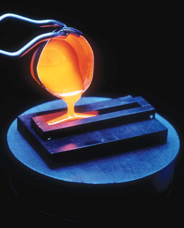
First, you don’t put the waste in any soluble or liquid form down in a geological repository. You make a solid waste matrix that is extremely resistant to any kind of corrosion or dissolution. The spent fuel is in the form of small ceramic pellets, and these have been in the reactor at hundreds of degrees for several years. They are very tough. You can dispose of these directly or else reprocess them to extract the radioactive nuclides, which are then mixed in a melter with glass so that you end up with these cylinders of black glass with the radioactive materials embedded in them. According to the best predictions that scientists can make, this glass takes more than 10,000 years to dissolve. You encase this glass in a stainless-steel sheath and put it in a copper container. Underground, where there is very little oxygen, copper acts like a noble metal, so these containers can last for more than 10,000 years. But you don’t stop there. The container goes into the repository at a depth of some hundreds of metres in a hard rock like a granite, a clay or salt. There it is surrounded by another barrier, which is often a special water-tight material called bentonite clay, that separates it from the host rock. So there’s a rock layer, a clay layer, a metal canister and inside that we have the waste matrix.

Photo of radioactive material being mixed with molten glass for storage

Where can nuclear waste management technology improve?

The most physics-oriented option is transmutation. If you irradiate long-lived radionuclides you can break them down into shorter-lived radionuclides. Many people would like to see a system where the radionuclide mix that comes out of a nuclear reactor would be treated. So you would separate it out into all its components. The useful ones, such as the much-maligned plutonium, can go straight into a reactor as fuel, but all of the other ones, almost without exception, can be transmuted if you strongly irradiate them. You can do this in a reactor, but it’s not easy in the light-water reactors that are prevalent today. Various organizations, including the Bill & Melinda Gates Foundation, are supporting other reactor types, such as fast reactors and small modular reactors, which can transmute much more of the waste than is currently done. You can also transmute them in a particle accelerator. Transmutation – either reactor driven or accelerator driven – is often pointed to as something that would change the face of radioactive waste management in the far future.

How far away are we from this?

Scientifically, no distance. But to upscale the technology so that it can be done economically and safely is quite far off, if it ever happens. It would costs loads of money and any further manipulation or treatment that you do of these highly radioactive materials would mean that process workers would be exposed to some level of radiation. Then you have an ethical question: how much extra radiation should I be prepared to give a process worker today to save tiny potential radiation doses to people thousands of years in the future?

The other challenge that bothers me is in the remediation and cleanup area. When sites get radioactively contaminated, you can have large areas that will never be safe for people to live on unless you do something clever. There are lots of interesting technologies – hydrological, geochemical and physical – being tried to clean up contaminated sites or sites where there have been accidents. The most recent striking example is at Fukushima in Japan, which following the 2011 earthquake, tsunami and reactor accident will be a mess for decades to come. It’s difficult to clean up a reactor if you don’t know what’s inside it, and it’s difficult to approach them because there’s molten fuel in there. One recent development that I think is really smart is to use muon technology as a remote sensing tool: if you can measure the flux of muons, you can use them like an X-ray to see an image of the melted fuel (corium), and try to get a sense of the scale of the problem.

What’s next for you?

I have been involved for many years in promoting the concept that not every country has to implement its own geological repository. We normally use two words when discussing waste disposal challenges: “safe”, meaning radiological and environmental safety, and “secure”, meaning safety against the deliberate misuse of the material. Despite setbacks, nuclear power is expanding globally. If you think of a potential future where instead of having 10–11 technologically advanced countries with advanced nuclear programmes you instead have 30–40 newcomer countries, each with one or two nuclear power plants, then this hazardous material will be sitting around the world in many locations. One of the ways to keep that material safer and more secure is to concentrate it in fewer, very well completed facilities. A large part of my life is devoted to developing this concept of multinational disposal.

Copyright © 2026 by IOP Publishing Ltd and individual contributors