The electrical conductance at different locations on individual atoms has been measured by scientists in Japan. The experiment involved adding and removing electrons from atoms on a surface by using a scanning tunnelling microscope (STM). The technique could also be used to measure the distribution of charge in superconductors, as well as to study magnetic interactions on very small length scales.
An STM builds up an image of a surface by using an atomically sharp tip to inject or withdraw electronic charge. The tip is scanned across the surface at a height of less than 1 nm, and the position of the tip can be controlled in 3D with picometre precision. As a result, STMs can produce images of individual atoms on surfaces, and have also been used to measure atomic-scale phenomena such as the quantization of conductance.
In this latest work, Huwon Kim and Yukio Hasegawa of the University of Tokyo used a state-of-the-art STM to study the surface of lead in an ultrahigh vacuum and a just a few degrees above absolute-zero. They found that when the distance between the needle and the surface was relatively large (about 100 pm), the conductance decayed exponentially with this distance. This is exactly what is expected from an electric current created by quantum tunnelling. Also, the same decay was measured when the needle was directly above an atom and when it was above a gap between two or more atoms.
Atomic skimming
When the needle was brought closer to the surface, the conductance started to increase faster than expected if tunnelling were involved. However, this increase only occurs when the needle is directly above an atom. This, say the researchers, is because the needle skims the surface of the lead, putting it in direct contact with the top of each atom. This allows electrons to move more freely between tip and atom, thereby boosting the conductance. However, when the tip is over a gap between atoms, electrons can only be exchanged via quantum tunnelling.
When the needle is brought closer still – actually pressing into the surface – the reverse effect on conductance is seen. The conductance is highest when the needle is pressed into a gap between atoms, rather than into a single atom. The researchers believe this may be because when in a gap, the tip has access to electrons from all of the neighbouring atoms. However, when the tip is touching a single atom, it can only interact directly with electrons in that one atom. Nevertheless, says Hasegawa, studies by theorists will be required to clarify exactly what is going on. “Our basic conclusion is that we measure the conductance at the sites,” he says.
Probing the superconducting gap
This detailed understanding of the variable concentration of electronic charge around and between atoms may prove to be important in nanotechnology because it should aid the design and optimization of atomic-scale electronic devices. The researchers themselves, however, are interested in superconductivity. Lead becomes a superconductor at temperatures below 7.2 K, and their experiment was carried out at 2.1 K. Although the material would have been a superconductor during the experiment, the observations were made in a region of the energy spectrum where this would have made no difference. Now, however, the researchers are preparing a paper describing how they have used the technique to look at electrons in the so-calledsuperconducting gap, in the hope that this will provide insights into the nanoscale behaviour of electrons in superconductors.
Laurent Limot of the Institute of Physics and Chemistry of Materials of Strasbourg, France, commends the researchers, but points out that the technique is “not completely new”, because two papers in 2011 looked at the charge distribution around atoms, one in gold and one in C60 molecules. Nevertheless, he says, the researchers have shown the differences in conductivity at different sites much more solidly than previous work. As well as studying superconductivity, says Limot, one can envisage using a ferromagnetic tip to look at nanoscale magnetic interactions. This would be useful for developing spintronic devices that use the magnetic spin of the electron to store and process information.
Golden future – the second phase of Singapore’s giant Fusionopolis R&D centre.
By Robert P Crease in Singapore
I’ve landed in Singapore shortly before the 50th anniversary of the nation’s independence – Sunday 9 August is the official date. The event that brought me was a conference entitled “60 Years of Yang–Mills Gauge Field Theories”, the opening day of which on Monday 25 May featured speeches by C N Yang, who shared the 1957 Nobel Prize for Physics, as well as David Gross – the 2004 Nobel-prize winner. I spoke on Wednesday morning.
But the conference isn’t the only physics-related event scheduled in Singapore’s jubilee year. Another is the opening of Fusionopolis II, the second phase of an innovative research and development (R&D) hub funded by the government’s Agency for Science and Technology Research (A*STAR). Phase one opened seven years ago – you can relive Physics World news editor Michael Banks’s experiences here; phase two is slated to open on 19 October. The initiative aims to supercharge Singapore’s research ecology by putting in close proximity materials-science research institutes, industrial research centres, and an international collection of eminent universities.
Take Tom Lubensky, a condensed-matter physicist at the University of Pennsylvania in the US. He had been trying to get his colleague Charles Kane to listen to him, but Kane wasn’t having any of it. They inhabit offices on the same corridor of the Department of Physics and Astronomy at Pennsylvania and have collaborated on arcane problems in the past, but their work typically keeps them separated by many orders of magnitude. Lubensky focuses on “soft” materials, such as complex fluids and liquid crystals, which keep him in a mechanical, Newtonian world. Kane toils in a much smaller domain. He studies the electronic properties of solids and is more likely to interact with materials with exotic quantum behaviour.
This time round, Lubensky had been investigating a certain class of lattice that can have movement at the edges – but not in the bulk of the material. The idea that the edge of a material would behave differently from its interior reminded Lubensky of “topological insulators” – materials first discovered about 10 years ago in which electrons can flow easily along the surface but are stopped dead in their tracks in their bulk. But in the autumn of 2012 when Lubensky wandered down the corridor to tell Kane he had seen a connection between the mechanical vibrations of lattices and the quantum behaviour of exotic electronic systems, his colleague remained sceptical.
Lubensky told Kane he suspected that the dynamical matrix – which provides a mathematical description of all the possible motions of a lattice – looked similar to a description of how charge flows on a topological insulator. However, Lubensky couldn’t see the path from one concept to the other. “I went into that discussion with the bias that what Tom was doing had nothing to do with what I was doing,” recalls Kane. “We work in very different fields.” Kane simply couldn’t see a connection – at least not at first. He spent his time solving the Schrödinger equation, which has a single time derivative. Lubensky worked with Newton’s equations, which are second-order in time.
The two physicists could not have been farther apart, at least in terms of condensed matter, and Kane doubted they would find any link between the particular lattices he was studying and quantum electronics. Still, Lubensky persisted and Kane finally agreed to hear him out. “When we sat down and started talking together,” says Kane, “I began to appreciate how similar the two were. Tom already understood that in the back of his mind.” And so a collaboration emerged, in which the two physicists not only developed connections between the mechanical behaviour of this class of lattice and topological insulators, but also with other exotic electronic systems, such as “quantum Hall fluids” – 2D systems in which the electrical conductance is quantized.
Lattice work
A lattice is a tried-and-tested workhorse in any condensed-matter physicist’s toolbox. It’s usually represented as a 2D grid or 3D array, in which balls are linked by springs in periodic, repeating patterns. Its power lies in its simplicity: a lattice can be used to model everything from atoms arranged in crystals to the bonds that hold long-chain polymers together. Lattices have been used to explore how structures behave after being compressed, pushed, pulled, twisted or otherwise tortured. They’re useful at every order of magnitude, both to study how a material withstands forces and under what conditions it fails.
1 Floppy or not
(a) A 2D lattice made from sets of four points connected by springs will change its geometry when perturbed. (b) But adding springs along the diagonals will lead to the lattice regaining its shape when the perturbing force is removed.
Lattices can be rigid, which means the points can be wiggled but the structure won’t change. They can, however, also have “floppy” modes, which means that slight perturbations can cause a mode to “flop” with minimal energy – leading to big changes in the structure. Imagine, for example, a square 2D lattice with every set of four points connected by four springs (figure 1). Push gently on one point and you can change the geometry of the lattice, turning it into a parallelogram or even, with further pushing, collapsing it down to a straight line. But now imagine adding springs to the square lattice along the diagonals. After a small push on one of the corners, the lattice will return to its original shape. By adding the two springs, the lattice is no longer floppy but is now stable and rigid. Whether a lattice has floppy modes or not depends on the balance between degrees of freedom – how its points can move – and the number of bonds, which restrict that motion.
Lubensky had been particularly interested in lattices that are on the verge of mechanical collapse. He refers to these as “Maxwell lattices”, in honour of the Scottish physicist James Clerk Maxwell, who in 1865 laid out the conditions under which a network would be rigid. According to Maxwell, a lattice cannot be rigid unless the number of constraints equals or exceeds the degrees of freedom. In particular, the average number of point-to-point connections in a rigid lattice must be at least twice the number of dimensions. So in a 2D lattice, the average number of connections must be at least four. A Maxwell lattice is rigid, but just barely: Its average number of connections is exactly twice the number of dimensions.
2 Kagome baskets
(a) Kagome or basket-weave lattice with four connections per site; (b) the twisted kagome lattice, also with four connections per site obtained from the kagome lattice by counter-rotating triangles about shared sites.
Examples of Maxwell lattices in 2D (see figure 2 and 3) include the kagome lattice, named after a pattern found in a type of Japanese basket. There is also a “twisted” kagome lattice, obtained by counter-rotating corner-sharing triangles of the kagome lattice.
Researchers use such lattices to analyse mechanical instability – where the lattices fail – for a wide range of systems, from architecture to biological networks. They’ve also been used to predict the point at which spheres are packed so closely together that they become rigid. This “jamming threshold” can be observed in sand: if you run your fingers through lightly packed sand, the grains flow easily, but if you try to move your fingers through hard-packed sand, it remains locked in place and resists invasion. Geometry in such systems trumps composition: the material itself matters less than how the nodes and bonds that make it up are arranged.
3 Model approach
Vincenzo Vitelli and colleagues at the University of Leiden created physical models of floppy lattices. This model is a mechanical analogue ofwhat happens to the nodes (white dots) at the border of a lattice with floppy modes. At one end, the node can be wiggled back and forth, at the other end it’s stuck.
Floppy at the fringes
Lubensky was interested in lattices that are stable – but only just. But then he and his colleagues made a surprising observation. They found that the simple twist that produces a twisted kagome isn’t just a curious change of geometry. It resulted in a drastic change. A conventional kagome lattice may have floppy modes in its bulk, but the twisted lattice becomes “gapped” – which means those floppy modes are prohibited in the bulk.
This transformation of surface modes reminded Lubensky of the appearance of surface electronic states that appear when the bulk electronic modes of a topological insulator develop a “gap” – that is, states of energy that are prohibited in the material. In the lattice, that gap relates to floppy modes; in topological insulators, it relates to the movement of electrons. That’s why Lubensky went to see Kane – he was searching for a connection between the two problems. After they’d talked, Kane mulled over the dynamical matrix and saw what Lubensky was talking about. Something did seem familiar to him: the dynamical matrix almost looked like an operator. In fact, it looked a lot like the Hamiltonian of the surface states of a topological insulator, except that it lacked the “valence band” characteristic of an insulator.
Undoubtedly like many moments in history that have pushed a field forward, Kane found a solution just before he drifted off to sleep one night in December 2012. “I was lying in bed at home, trying to think about this, and realized after some effort that I knew how to do it,” Kane recalls. “I wrote to Tom the next day and said I could turn it into a problem I knew how to solve.” In hindsight, Kane says, the approach seems almost obvious. In fact, it was buried in a previous paper by Lubensky and other collaborators (2010 Phys. Rev. Lett.104 085504). “If you go back and look at that paper, it really does smell like the same kind of topological boundary modes that occur in electronics systems.”
Kane thought that he could break down the matrix by effectively taking the square root of it, an approach once used by Paul Dirac to unify quantum theory with special relativity. Kane and Lubensky ultimately produced a result that, when regarded as a Hamiltonian, also described a topological insulator. The pair reported the connection between the two fields in the January 2014 issue of Nature Physics (10 39) – a paper that attracted the attention of Vincenzo Vitelli, a soft-matter theorist at the University of Leiden in the Netherlands.
LEGO heads
“One thing that’s fascinating about Charlie and Tom is the combination of research areas,” says Vitelli. “Charlie is a leading expert on electronic materials, and Tom has worked on many things, including soft-matter materials. Their Nature Physics paper was a bridge between those areas.” But when he first read the article, Vitelli’s immediate thought was that he wanted to see the phenomenon for himself. “In line with the spirit of the soft-matter community, the first question that came to our minds was: ‘Can you literally bring this difficult concept to your fingertips? Can we build this bridge to understanding?’ ”
Despite having been trained as a theorist, Vitelli believes in the power of playing with and learning from real, physical objects, such as LEGO bricks – a stack of which he keeps in his office. He and his team used various building blocks, which he describes as “LEGO on steroids”, to build a physical representation of the lattice with the same properties as those described by Lubensky and Kane. To the outsider, their contraption looks like a complicated series of transparent “flippers” of the kind found in pinball machines, connected by springs and rods to each other – and to a bar that holds it all together.
The resulting chain, based on Kane and Lubensky’s description, might look curious but it behaves like their lattice and aptly demonstrates the predicted floppy modes at the border (figure 3). Vitelli’s models are, in other words, a mechanical analogue for what happens to electrons in a topological insulator; to watch videos of the models in action is to witness a quantum effect on the macro scale. “They’re really quite remarkable because they have the property we discussed,” says Lubensky. “At one end, you can wiggle the bond the back and forth, and at the other end it’s stuck.”
Vitelli kept going and found that with some minor adjustments – and by tilting the chain up on its end – a similar device could actually conduct the mechanical motion along its length, propelled by gravity. In a video of the device (see below), one can see the “kink” at the edge travel, flipper by flipper, through the chain. Vitelli called this phenomenon a “flipper soliton” – a wave-like phenomenon that transports energy along the length. So whereas Lubensky and Kane had predicted the floppy mode would remain localized on the border and act as an insulator, Vitelli’s mechanical lattice – this chain of flippers – showed that the mode can travel through the bulk, which therefore acts as a conductor, too.
Theoretically, the chain behaved as though the edge mode moved the entire structure, which is a key difference between the quantum and classical states. When you push on an electron, in contrast, it doesn’t disturb the whole structure underneath. Vitelli and his co-authors therefore went searching for the origins of the phenomenon, which centred on the fact that Lubensky and Kane had limited their work to using linear elasticity. Once you treat the lattice as a nonlinear system, however, the soliton appears. The behaviour of the soliton, in other words, is built into the topology of the lattice itself.
Making metamaterials
The observation that floppy modes can in fact reach the interior of a lattice suggests yet another direction for research. “It tells you that you can use defects in a positive way,” says Vitelli. In a paper published earlier this year (Nature Phys. 10.1038/nphys3185), Vitelli and his team showed that it is possible in practice to actually build such modes – as defects – into the fabric of structures like the Kagome lattice studied by Lubensky and Kane.
Once again, the Dutch physicists turned to LEGO-like building blocks to demonstrate the phenomenon on a macroscopic scale. Using physical models in 2D, they showed that these defects, just as with the floppy edge modes, could be constructed to remain localized or to propagate as vibrations through the lattice. And like the floppy edge modes, these defects behaved like mechanical analogues of topological insulators. But what is interesting is that a material constructed to include these sorts of topologically protected defects can be classified as a “metamaterial”.
Metamaterials are artificially engineered substances – typically built from collections of rods or rings – with properties that arise from how the component parts are put together, not the composition of those parts themselves. It’s a case of geometry, not chemistry, ruling the roost. Metamaterials are most familiar in the pursuit of cloaking devices that can hide an object from, say, incoming light or sound, but they are essentially just a network of nodes connected by links – a lattice in other words. In a recent paper published with Jayson Palouse and Anne Meeussen (arXiv:1502.03396), Vitelli has described a metamaterial in which buckling regions are sculpted into its topology. “We can control the states of self stress, depending on where we put the defects,” he says.
Metamaterials such as those described by Vitelli and his team might be used to store data, provided they can be made very small. At larger scales, such substances might even lead to new building materials that can only fail in predictable ways. But perhaps the most promising use for such a material is in robotics or “smart” metamaterials, where the floppy modes could be activated by tiny built-in motors. (Right now, the solitons only arise when someone pushes on an edge of the lattice.)
Vitelli points out that no-one knows where the research is heading. “Nobody has the crystal ball,” he quips. The groundwork for mechanical-quantum analogues, in the form of floppy modes, has been laid, and now researchers face the challenge of showing that it might be useful. “We need one very cool application,” says Vitelli. “The material has been shown to exist, he says, “but now we need to go beyond that. We have to show that this material does something better than something else.”
Those dreams are a long way from the original work of Lubensky. In fact, Lubensky thinks that he and Kane might have found their connection even sooner if condensed-matter physicists didn’t divide themselves so strongly along quantum and classical lines. “In the end, we were talking about the same underlying mathematics,” he says. Of course, physicists have been studying for decades how lattices hold and fail, but Kane and Lubensky do appear to have established the foundation for a new avenue of investigation. All of which proves the power of persistence.
While proton therapy is a very promising way of treating cancer, researchers are keen to ensure that the beams have indeed hit their target. While this could be achieved using positron emission tomography (PET scanning), it needs to be done immediately after the therapy has been carried out, before the radioactivity within the patient decays and becomes distorted by biological “washout”. Now, researchers in the US have developed a more accurate extrapolation of radioisotope distributions at the time of irradiation using a kinetic model applied to dynamic PET scans done soon after irradiation. According to the researchers, their approach provides a patient-specific alternative to generic “washout factors” derived from animal studies, which have limited accuracy.
Proton therapy makes use of extremely precise proton beams that are directed at tumours to destroy them while avoiding any surrounding healthy tissue. PET shows promise as a means to verify proton-therapy delivery, by imaging positron emitters generated by a proton beam. However, in vivo radioisotope distributions are distorted by biological washout, which varies between patients and increases with the delay between treatment and scanning, thus presenting a major challenge.
A kinetic model
The model – developed by Kira Grogg of Massachusetts General Hospital (MGH), together with colleagues from MGH, Harvard Medical School and Yonsei University in Wonju, South Korea – describes the variation in concentration of activity for a given molecule containing a positron emitter, taking into account both the isotopes that are generated during the therapy and their subsequent decay or clearance. This clearance is determined by both physical decay and biological washout that varies according to the radioisotope’s molecular form.
“Our method can be used to improve PET monitoring of proton therapy by removing biological factors that affect the comparison of delivered to expected distributions,” says Grogg. “This is a step in making the process more accurate and reliable, and should eliminate the need for empirical washout factors when imaging is done soon after treatment.”
Several radioisotopes are generated during irradiation – including nitrogen-13 (13N) and carbon-11 (11C) – in a variety of molecular forms. However, 80% of the PET signal originates from oxygen-15 (15O), and water dominates the body’s composition. Consequently, the researchers’ model assumes a dominant contribution from the 15O present in water molecules with a correction for other radiolabelled molecules. By fitting the model with dynamic PET data, 15O production and clearance can be carefully and accurately determined.
Phantom and animal validations
Grogg and colleagues first tested their model for the simple case of a “phantom” (a specially designed object used in medical imaging to study, evaluate and tune the performance of imaging techniques), without the presence of biological washout. The phantom, made up of three materials with known elemental compositions, was irradiated with a passively scattered proton field and promptly imaged with a mobile PET scanner for 30 minutes with 1 minute frames. The team found that the fitted model correctly predicted physical decay constants for 15O, 13N and 11C.
Biological washout was introduced by scanning the thigh of a live rabbit. The scan was then repeated after the animal was sacrificed, leaving only physical decay. Using the model, the two scenarios gave 15O production rates within 2% of one another and the clearance rate was also consistent, further validating the model.
“Currently, we are collecting patient images with our mobile PET/CT, which we can bring into the treatment room,” says Grogg of ongoing research at MGH. “We hope to demonstrate the feasibility of our method in human studies, and, in particular, show an improvement in the comparison between measured and simulated PET images, as an initial step to clinical implementation.”
For full clinical implementation, a dedicated in-room scanner that reduces the time between treatment and imaging is needed, ideally using a partial-ring detector to acquire data during treatment, or a full-ring detector that can be moved into place immediately following irradiation, says Grogg.
Think back to the last time you took a physics exam. Was your heart racing? Did you gulp when you realized that you had no idea – really no idea at all – how to solve the first problem? And then, just as the fear threatened to engulf you, did you hear a tiny, confident voice in the back of your head saying, “Hold on a minute, what if I do this…”? If any of these experiences sound familiar to you – and if they inspire a certain wry fondness rather than a panic attack – then you need to add Physics on Your Feet to your library. Subtitled “Ninety Minutes of Shame but a PhD for the Rest of Your Life,” the book is a collection of the best questions posed to physics students at the University of California, Berkeley, during the oral exams that were, until 2010, part of the standard postgraduate training programme. The curators of this collection, Dmitry Budker and Alexander Sushkov, have been on both sides of the examiner/examinee divide (both of them earned their PhDs at Berkeley, and Budker is now a physics professor there), and the questions that appear in their book are both fiendish and fascinating. A few can be solved using only high-school-level physics, carefully applied. But be warned: some problems that seem simple actually contain hidden depths, and a few of them might even lead to heated debates in departmental tea rooms and company cafes as senior physicists argue over the answers. (Try the one about tides during a solar eclipse on an unsuspecting friend.) Budker and Sushkov have supplied their own solutions to each of the problems, but they do not claim that these are the only answers; some of the questions are, in any case, open-ended enough to permit several possible approaches. Readers who work their way through all of these questions won’t get a PhD for doing so, but they will get a much better appreciation for the richness of physics as a discipline.
2015 Oxford University Press £19.99pb 224pp
Going deep underground
The inside of the Earth is intimately connected to the universe outside it. Many of the treasures hidden there originated in distant stars and galaxies, and theories of our solar system’s very early years, when the Earth and its neighbours coalesced, can also tell us much about our planet’s present composition. This deep connection helps explain why an astronomer, David Whitehouse, has chosen to base his latest book on the Earth’s interior. Journey to the Centre of the Earth takes its title from Jules Verne’s novel, which celebrates its 150th anniversary this year, and, like Verne, Whitehouse has a magpie’s eye for interesting facts and stories. Perhaps the oddest of these little nuggets is the revelation that the brand name Bovril comes from Vril, an early science-fiction novel about a subterranean race of super-humans. None of these tales of the deep Earth is told in very much detail, though, which is sometimes a pity. Humankind’s various attempts to drill through the Earth’s crust and into the mantle, for example, occupy a mere eight pages in Journey, yet it is clear from Whitehouse’s description that an entire book could be written about the Kola Superdeep project alone. This effort lasted for 25 years and produced a 12 km-deep borehole before technical and monetary difficulties ended operations, and Whitehouse calls it “one of the great scientific projects of the 20th century”. Perhaps someone will write a book about it one day, but in the meantime, there is plenty to enjoy in this one. As Whitehouse puts it, “if you want strangeness and surprises, look below”.
For nearly three decades, physicists have been unable to answer a seemingly simple question: where does proton spin come from? Adding up the spins of the three quarks that make up the proton seems, in principle, straightforward, but physicists have been struggling with a strange problem: the sum of the spins of its three quarks is much less than the spin of the proton itself.
Known as the “spin crisis”, the topic appears as the cover story of the June 2015 issue of Physics World, which is out now in print and digital formats. In the feature article, science writer Edwin Cartlidge examines the origins of the problem – and whether new experiments could mean we are about to solve it at last.
If you’re a member of the Institute of Physics (IOP), you can get immediate access to the feature with the digital edition of the magazine on your desktop via MyIOP.org or on any iOS or Android smartphone or tablet via the Physics World app, available from the App Store and Google Play. If you’re not yet in the IOP, you can join as an IOPimember for just £15, €20 or $25 a year to get full digital access to Physics World.
The issue also includes a great Lateral Thoughts article by Felix Flicker that’ll have you twisting and bending your arms as you try to follow what he’s on about.
Jim Parsons and UCLA alumna Mayim Bialik from The Big Bang Theory TV show. (Courtesy: Warner Bros Entertainment Inc.)
It’s not often that one can say that watching TV may help your future career as a scientist, but today, after the hit US TV show The Big Bang Theory announced a scholarship for STEM students at the University of California, Los Angeles (UCLA), it may be possible. The show, revolves around a group of young scientists – mainly physicists, but also an engineer, a microbiologist and a neuroscientist – making it a science-heavy show. Indeed, we at Physics World have delved into the secrets of the show’s success and talked to one of its scientific advisers. Now, the sitcom’s co-creator, cast and crew have announced a scholarship fund at UCLA to provide financial aid to undergraduate students pursuing degrees in science, technology, engineering and mathematics. The show’s executive producer, Chuck Lorrie, told the Deadline website that “when we first discussed it, we realized that when Big Bang started, this freshman class were 10 year olds”, adding that “some of them grew up watching the show, and maybe the show had influence on some of them choosing to pursue science as a lifetime goal. Wouldn’t it be great if we can help.” For this academic year, 20 “Big Bang Theory scholars” will be picked to receive financial assistance, with five new scholars each year from now. You can read more about it on the BBC website.
A new kind of silicon photodetector invented by physicists in Canada and the UK should help to ensure that the Internet does not grind to a halt, as people share and download ever-more online data. The device, which could be built using existing chip-fabrication techniques, would ease the pressure on the Web’s data centres by opening up a new frequency range in optical communications.
Ever-greater use of social media, video streaming and other data-heavy applications is causing a rapid rise in Internet use. US technology company Cisco Systems says that worldwide Internet traffic increased more than five-fold between 2008 and 2013, and is set to rise by another factor of three by 2018. This apparently insatiable appetite for online services puts pressure on the hardware that makes up the Internet, and in particular on the huge data centres that route bits and bytes between computers across the globe.
Rising demand
Until now, the companies operating such data centres have tended to use electrical wiring to link the thousands of servers that they employ, but many are now replacing that wiring with fibre-optic cables – these have a number of advantages over the copper variety, including lower losses over long distances, the fact that they do not pick up electromagnetic interference and, crucially, their far greater bandwidth. However, says Andrew Knights of McMaster University in Ontario, even current fibre technology might be swamped by rising user demand within a decade or two.
In the latest work, Knights, together with Jason Ackert and colleagues at McMaster and also the University of Southampton in the UK, have built and tested a photodetector – a device that converts the pulses of light sent down a fibre-optic cable into electrical signals that serve as input to computer processors – that is designed to meet that demand by increasing the range of wavelengths that can be used to send data. Most current cables work at bands centred on 1.3 or 1.5 μm, and transmit data over about 100 different channels within each band – with each channel corresponding to a slightly different wavelength. The new device would, the researchers say, help to open up at least another 100 channels by operating at longer wavelengths, exploiting a band lying in the mid-infrared region at around 2 μm.
Photodetectors operating at mid-infrared wavelengths have already been built from materials other than silicon, notes Knights. But these rival devices, he says, suffer from drawbacks. Germanium–tin detectors, for example, operate too slowly, and produce quite small electrical currents, while detectors based on III–V semiconductors are difficult to integrate into silicon circuitry.
Ion defects
The new device consists of a 3 μm-wide strip of silicon that has a thickness of 220 nm at its centre and just 90 nm at its edges, deposited on a substrate of silicon dioxide. Ordinarily, such a device would serve as a waveguide that is transparent to mid-infrared radiation, but the Anglo-Canadian group inserted ions into the silicon to introduce defects into the lattice structure. These defects result in electronic states within the silicon’s band gap, which allow low-energy mid-infrared photons to excite electron–hole pairs and so generate a measurable photocurrent.
Knights and co-workers have shown that their device generates a reliable electrical response at wavelengths between 1.96 and 2.5 μm, albeit with a lower sensitivity than similar silicon detectors operating at 1.55 μm. They also exposed the device to the output of a 1.96 μm laser diode, showing that at this wavelength it could operate without errors at speeds of greater than 20 gigabits per second – more than any other photodetector at this wavelength.
Easy fabrication
The researchers have also shown that their design could be realized using standard CMOS fabrication, having had their prototype device manufactured at a commercial foundry in Singapore. This is crucial, they say, because it means being able to take advantage of the existing vast infrastructure used to fabricate microchips, so lowering costs significantly. Indeed, waveguides, multiplexers and most of the other components needed for optical-fibre communication in this new frequency band have already been built from silicon by other research groups. “We have shown that our device is fast, that it operates at the right wavelength, and that it is compatible with silicon fabrication,” says Knights. “If you put these things together, that is a major breakthrough.”
Knights points out that there is unlikely to be a mass market for this device until Internet traffic has grown accordingly. But he is confident that the market will materialize. “We can place this in the toolbox and it will be ready when needed,” he says.
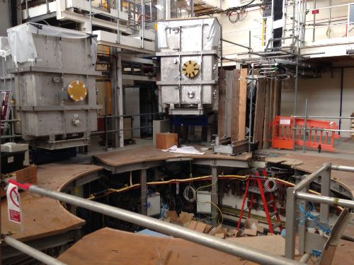
Owned and operated by the United Kingdom Atomic Energy Authority, the CCFE is already home to the Joint European Torus (JET) tokamak, which in 2011 underwent a £60m upgrade programme that involved replacing the carbon tiles in the inner reactor wall with beryllium and tungsten. The purpose of this retrofit was to test the materials that are to be used in the ITER fusion experiment, which is currently being built in Cadarache, France.
Culham is also home to the Mega Amp Spherical Tokamak (MAST). MAST has a spherical plasma, shaped much like a cored-out apple, whereas JET (and ITER) has a doughnut-shaped plasma. A spherical tokamak allows for a much more compact – and cheaper – device and it is hoped that this kind of tokamak could one day be used as a potential fusion reactor.
MAST is currently half-way through a £45m upgrade of its own that will be complete sometime next year. The upgrade is a major overhaul of the facility that will see the tokamak given a new “divertor”, which extracts the waste fuel from fusion. Called “Super-X”, it is hoped that the new divertor could even be used in a future demonstration fusion plant – dubbed DEMO.
Yesterday I was given a tour of the MAST construction site, which involved donning the customary hard hat and overalls. The level of the overhaul is impressive, and it becomes immediately clear that this is not just a minor upgrade, but almost like building a new machine.
Before the MAST tour I spoke to Steve Cowley, director of the CCFE, who says that an actual fusion reactor delivering energy to the grid could even be in some way a combination of a standard fusion tokamak like ITER and a spherical tokamak. This, according to Cowley, makes the experiments that will be run with the MAST upgrade important. “This is a world-class experiment,” notes Cowley, “and one of the biggest physical-sciences facilities in the UK.”
Be sure to keep an eye out for a piece about the MAST upgrade in an upcoming issue of Physics World.
Construction of the Thirty Meter Telescope (TMT), which has been delayed for months following protests by native Hawaiians, has taken a key step towards restarting. At a press conference on 26 May, governor of Hawaii David Ige noted that the TMT – to be built on the country’s highest peak, Mauna Kea – has the right to proceed, and that all of the necessary permits for the observatory have been obtained. Yet, he criticized how the University of Hawaii has managed the land on Mauna Kea, outlining 10 improvements – some recommended and some required – for how the university uses the mountain.
Since 1968 the University of Hawaii has leased more than 44.5 km2 of land on Mauna Kea from the Hawaiian Department of Land and Natural Resources (DLNR) for scientific purposes, with the highest 2.1 km2 devoted to astronomy research. The top of Mauna Kea is already home to 13 telescopes, and the TMT will be the largest and most powerful instrument when it is operational in 2023. The telescope’s 30 m primary mirror will be made of 492 hexagonal segments, and a structure 66 m wide and 56 m tall will house the telescope. The TMT will sit on a plateau about 500 feet below the summit, a location picked to reduce the telescope’s visibility from the majority of the island.
Fewer telescopes
Construction of the TMT had been halted in early April following protests by native Hawaiians, who see its construction on Mauna Kea as desecration of their spiritual and cultural pinnacle. Over the past eight weeks, Ige has mostly stayed quiet regarding the protests, but now, along with giving permission for construction to restart, he requests that the university returns all of the land not used for astronomy to the jurisdiction of the DLNR. He also says that the University of Hawaii should begin decommissioning one telescope later this year with at least one-quarter of the remainder to be completely dismantled by the time the TMT is operational, with each site to be returned to its natural state.
One of those affected could be the Caltech Submillimeter Observatory. It was already slated to be dismantled, starting in 2016, but that may now be brought forward. Yet according to cosmologist Asantha Cooray of the University of California, Irvine, decommissioning a telescope is far from simple, and takes at least a couple of years. He says that the University of Hawaii – rather than the astronomical community – will likely decide which other three telescopes will be removed.
Cultural contribution
Ige also announced that the state government would work to change how the mountain is managed, and that it will form the Mauna Kea Cultural Council. This group will review the subleases to observatories, all proposed rules, and any preparatory work regarding the environmental impact of telescopes on the mountain. Thayne Currie, an astronomer with the Subaru Telescope on Mauna Kea who has also worked at other observatories on the site, says that this new council is a step in the right direction, provided that it “is tasked with not just simply receiving messages from the native Hawaiian community, but really considering their mission to try as much as they can to make sure their concerns are reflected in action”.
While the new rules will hit facilities on Mauna Kea, Ige, however, still believes that both science and culture should co-exist on the mountain. “Science has received most of the attention and has gotten way ahead of culture in our work on the mountain,” he says, adding that “the proper balance” between the two had been lost. In a statement, TMT members noted that “We are grateful to governor Ige for his leadership and his statement of support for TMT’s right to proceed. We will work with the framework he has put forth.”


 (a) A 2D lattice made from sets of four points connected by springs will change its geometry when perturbed. (b) But adding springs along the diagonals will lead to the lattice regaining its shape when the perturbing force is removed.
 (a) Kagome or basket-weave lattice with four connections per site; (b) the twisted kagome lattice, also with four connections per site obtained from the kagome lattice by counter-rotating triangles about shared sites.
  Vincenzo Vitelli and colleagues at the University of Leiden created physical models of floppy lattices. This model is a mechanical analogue of