It’s one of the biggest universities in the world with several hundred thousand students, but the Universidad Nacional Autonóma de México (UNAM) is certainly not the oldest. In fact, the first person to get a degree and PhD in physics at UNAM – Fernando Alba – is still alive. Aged 95, he studied at UNAM’s Institute of Physics shortly after it opened its doors in 1939.
When you visit an unfamiliar city, you can often discover some hidden gems by just wandering the streets with your eyes wide open. This is what happened to Physics World editor Matin Durrani and me yesterday here in Mexico City when we stumbled across the Museo de la Luz (Museum of Light) in the backstreets of the historic city centre.
Located in an old Jesuit college with a beautiful courtyard, the exhibits are spread over three floors covering a wide spectrum of themes, from human vision to the history of the theories of light. What I loved about the place is that it really did offer something for everyone. Too often I find that museums can be great for kids or great for the type of serious adult who loves to leaf through tea-stained archives. El Museo de la Luz manages to hit a sweet spot, being informative and interactive but not too whizz-bang – that is certainly not what I needed yesterday with this jetlag!
The delay in the construction of the Thirty Meter Telescope (TMT) on Hawaii’s tallest mountain, Mauna Kea, is continuing to cause turmoil within the astronomy community. First, the Office of Hawaiian Affairs (OHA) Board of Regents announced in April that it had withdrawn its support for the telescope. Then, last month, an e-mail forwarded to some 200 astronomy faculty, researchers and students sparked outrage when it claimed that the telescope was being “attacked by a horde of native Hawaiians”.
Construction of the TMT – featuring a primary mirror 30 m across that will be housed in a structure 66 m wide and 56 m tall – had been halted in early April, following protests by native Hawaiians. Mauna Kea is currently home to 13 telescopes, and TMT supporters maintain the newest and largest observatory will be constructed with care for the environment and the mountain’s cultural importance. TMT members say they have obtained all of the necessary permits for the observatory, and that they have the legal right to proceed. But indigenous Hawaiians claim that Mauna Kea – their spiritual and cultural pinnacle – is being desecrated, and a growing number of astronomers are now at odds with the project, too.
On 20 April, the situation became tense when an e-mail by University of California astronomer Sandra Faber to a group of astronomers – which was then forwarded to 200 astronomy faculty, researchers and students – sparked outrage. In the e-mail, Faber stated that the TMT is “in trouble, attacked by a horde of native Hawaiians who are lying”. Faber has since apologized.
Professional environment
On 6 May, Megan Urry, president of the American Astronomical Society (AAS), released a statement in which she underlined the diversity in the astronomical community. “I tell all of you, very clearly,” she wrote, “that racism is unacceptable, that referring to groups as monolithic is not acceptable, and that the AAS is firmly committed to an inclusive, welcoming, professional environment.” Urry added “Astronomers may have a range of opinions and perspectives on various matters, but we speak as one on the principle of respectful discourse at all times.”
Urry’s statement came a week after the OHA Board of Regents voted to rescind its 2009 decision to support Mauna Kea as the site of the TMT. The OHA is a public agency that is responsible for improving the well-being of native Hawaiians. The decision on 30 April, which followed some four hours of testimony, is a neutral stance because the board could have voted to oppose the construction – indeed, some were upset that it did not do so. The OHA board says that the neutral stance provides it with a bargaining chip of sorts in future negotiations regarding how Mauna Kea is used.
I don’t know about you, but my trick whenever flying halfway across the world is to shoehorn myself as fast as possible into the new time zone I’m in. Having travelled from the UK to Mexico City with my colleague James Dacey yesterday, that tactic seems to have worked…so far. After staying up till midnight following a mini-feast of fabulous spicy tacos at a nearby restaurant while a thunderstorm broke, I woke up on cue at 7 a.m. as dawn broke in one of the biggest urban areas in the world.
We’re both here to gather material for a Physics World special report on physics in Mexico, which is due out in September. Following fast on the heels of recent reports on India, Brazil, Korea, India (again), Japan and China, the report will shine a light on some of the exciting physics research going on in the country and highlight some of the challenges and opportunities the country’s physicists face, too.
Imagine that you were to visit a distant planet and find its surface blanketed with sophisticated machines. These machines sense and respond to their environment, diagnose and repair themselves, and create their own fuel from their surroundings. As a technology-savvy earthling, you would be incredulous to learn that the only value seen in such machines was to grind them up, process and eat them – yet this is precisely what we do every day. Plants on Earth possess all of these diverse functions and more, but only now are we beginning to consider the potential of plants for new technologies.
Augmented technology
The nascent field of “plant nanobionics” seeks to harness known properties of plants to augment or reinvent human technology. By treating living plants as technological platforms we can learn how to integrate nanoparticles with plant-based materials to impart novel functions to devices. Sensors in the form of plants could sample their environment through transpiration and report the result via radio-frequency signals, for example, or we can imagine self‑repairing, plant-based photonic devices that serve as communications networks. Plants even have their own power source – photosynthesis, which has the added benefit of consuming carbon dioxide – and are made of cheap materials that are naturally recyclable.
The possibilities of plant nanobionics are potentially far-reaching. A world in which materials repair themselves using sunlight or where buildings in cities act as active carbon sinks would be transformative. Nanoelectronic devices parasitically wired and integrated into a plant’s internal machinery could draw power, store energy and communicate sensory information relating to water stress, chemical exposure, nutrient stress or ambient illumination. How realistic is this vision? While there are definite limitations to plant nanobionics, this is a new field with much unexplored territory and scope for surprise.
Consider photosynthesis from an engineering perspective. A plant chloroplast (the photosynthetic engine of the organism) can produce sugars at an average rate of 40 µg per square centimetre per hour. That is equivalent to 10% of the energy stored in a watch battery each day – not enough to power your smartphone or tablet, but sufficient to drive an active radio-frequency identification circuit to export information, an electrochemical sensor to generate information, or a luminescent beacon for signalling.
The stems of plants, which transport sap from the roots to the leaves via a bundle of conduits each being 10–100 μm across, are another natural engineering marvel that could be exploited for devices. The electrolyte-containing conduits have an electrical conductivity of 0.5 millisiemens per centimetre, which is more than 30 times higher than that of silicon at room temperature, therefore providing channels for parallel communications from the ground to the tips of leaves.
Furthermore, pressure drops induced in the xylem from evaporating water inside leaves can reach values of more than –3 MPa. This is similar in magnitude to the pressure drops that power the entire field of microfluidic devices, which today are typically provided by bulky external pumps.
These are just a few examples that reveal the potential of plants as engineering materials, but there is much more infrastructure within the plant that could be tapped for applications. Plant nanobionics is distinct from the now well-established field of biomimetics, in which engineers learn from natural systems to create new synthetic materials, because it seeks to incorporate living plants into the final device. In plant systems, the use of nanotechnology for this purpose has no precedent.
Merging disciplines
Working at the intersection of plant physiology and nanotechnology, we became interested in plant nanobionics in 2010 thanks to a research project in which we studied plant self-repair mechanisms during photosynthesis. Our goal was to mimic such repair in synthetic devices, and we successfully built self-assembled photo-electrochemical devices by combining carbon nanotubes into a plant’s photosystem. However, the project motivated us to investigate whether we could exploit existing functions of the plant’s natural machinery – such as self-repair and the conversion of solar energy into fuels – to create high performance, self-repairing solar cells.
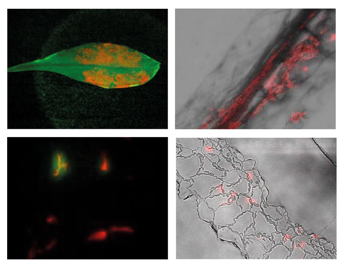
Last year we reported a series of new techniques that allow nanoparticles to be delivered and localized within living plants and plant organelles, and we were able to demonstrate several novel functions that could emerge as a result (Nature Materials13 400). Using extracted spinach chloroplasts and leaves from Arabidopsis plants, we found that single-walled carbon nanotubes (SWCNTs) augment both the light reactions of photosynthesis and biochemical detection functions in these species. Furthermore, we discovered that, under certain conditions, SWCNTs can be made to assemble within the chloroplast’s photosynthetic machinery, which has proven to be a powerful enabling technique.
Surprisingly, SWCNTs that are thousands of times longer than the thickness of a lipid bilayer penetrate the outer lipid envelopes of chloroplasts and are left trapped on the inside. Wrapped in highly charged molecules, the SWCNTs assemble within the chloroplast photosynthetic machinery via a mechanism we call lipid exchange envelope penetration (LEEP): the SWCNTs become coated with lipids that form the chloroplast envelopes, pulling nanotubes in as the membrane repairs itself and thereby trapping them inside. LEEP could potentially be used to make many new types of hybrid photosynthetic materials in plants, including those that absorb light at wavelengths across the electromagnetic spectrum or those that have chemo-protective capabilities against photo-damage. We demonstrated that SWCNTs can enhance the rates of photo-induced electron transport both in chloroplasts extracted from the plant-cell host and in leaves of living plants by up to 30% relative to controls.
The delivery of SWCNTs to living plants was performed by infiltration through the stomata, which are the pores that control gas exchange between leaves and the atmosphere. We also exploited this mechanism to deliver nano-sized particles of cerium oxide (known as “nanoceria”) inside chloroplasts, significantly reducing the levels of reactive oxygen species to values 28% lower than in control chloroplasts. Nanoceria particles act catalytically as potent scavengers of these damaging molecules, a bit like supercharged vitamin C, thus protecting the chloroplast protein complexes and significantly extending the lifetime of the plant.
We also showed that plants assembled with carbon nanotubes can act as chemical sensors that communicate by fluorescent signalling. These nanobionic plants report changes in the concentration of nitric oxide (a plant-signalling molecule and environmental pollutant) by modulating the near-infrared emission of nanoparticle sensors embedded within the leaf lamina. The modified plants are able to respond within seconds of exposure and are capable of detection sensitivities below one part per million in aqueous media. We envision such nanobionic plants replacing more expensive inorganic sensors based on electronics and plastics for the detection of explosives or environmental pollutants, for instance.
Merging materials In vivo fluorescent imaging of a plant that has been integrated with single-walled carbon nanotubes (red), showing their presence in: the leaf (top left), near leaf veins (top right), parenchyma cells (bottom left) and chloroplasts (bottom right). (Courtesy: Nature Materials)
The discovery that SWCNTs can assemble within a plant’s photosynthetic machinery raises the possibility of biocompatible electrodes patterned within and on the surfaces of leaves and stems. These could be interfaced with plant tissues to produce electrical circuits for computation, electrochemical detection of molecules inside the plant, or external communication. This merging of synthetic and natural infrastructures is one of the central visions of plant nanobionics. A laccase–glucose oxidase electrode pair, for example, creates a biofuel cell that could syphon off stored glucose to electrically power the circuits. This could allow the circuit to monitor the plant’s photosynthetic output directly by quantifying the sugars that are the main products of photosynthesis.
Monitoring other plant signals is similarly intriguing. Abscisic acid, for instance, is a hormone produced by roots in response to dry soil conditions that controls plant transpiration by closing the stomatal aperture. We can therefore imagine nanoelectronic circuits that respond to plant chemical signals and control the water content of their environment, for example by generating a radio-frequency signal that activates an irrigation device in response to water stress.
We can even consider incorporating plant systems directly into our own building materials to provide added functionality. Since chloroplasts can perform the basic function of converting sunlight and carbon dioxide into sugars even when they are removed from a living plant cell, materials containing transplanted chloroplasts could potentially capture unwanted carbon dioxide from the atmosphere. For this to be possible, however, we first need to prevent the natural degradation of the “naked” chloroplasts caused by reactive oxygen species and other mechanisms when they are removed from the plant cell. At the Massachussetts Institute of Technology we have recently been working on the concept of a “hyperstable chloroplast” as an engineering material, perhaps based on chemo-protective nanoparticles such as nanoceria.
Calling all physicists
Such visions might at first seem a bridge too far. Plant nanobionics requires interdisciplinary research teams and strong collaboration between plant scientists and nanotechnology researchers to make it reality, but there is a wealth of scientific knowledge and technological potential to be gained on the way towards this goal. Enhancing crop yields and the productivity of algae biofuel, or creating novel hybrid photovoltaic and optical communication materials, are already widely studied technological goals. But some applications, such as authentic plant cyborg tissue, require completely new avenues of exploration.
There are many different scientific and engineering challenges for plant nanobionics in the decade ahead. We have shown that nanoparticles introduced to a plant can be trafficked to the chloroplasts in leaves via vascular infusion, but what about directing other nanoparticles to other plant organs or tissues to boost or introduce additional functions? Does a given nanoparticle with particular properties and coatings affect its transport within the plant? Such questions are still poorly understood, but will help to develop plant biocompatible circuits and optical communication materials.
To bridge the world of electronics and plants, we also need to understand the physical limitations imposed by the plant. We have to determine, for example, how electromagnetic interactions within and between nanomaterials affect the way that visible, infrared or radio-frequency waves interact with living plants. As with every new technology, safety studies should also be thoroughly conducted before taking nanobionic plants outside the laboratory. Nanotoxicity studies demonstrate that the behaviour of nanomaterials in living tissue depends a lot on the surface chemistry, aspect ratio, nanoparticle size and other properties. While studies in this area will help engineers to design additional biocompatible materials for the plant interface, many nanobionic applications – such as those designed to replace or enhance silicon, plastic and metal devices for communications, photonics or self-powered systems – do not involve ingestible nanoparticles.
There are seemingly endless opportunities and challenges in using nanotechnology to enhance and exploit the diverse functions of plants. One certainty, however, is that plant nanobionics requires the engagement of multidisciplinary teams of plant biologists, chemists, engineers and physicists alike.
It is 50 years since Intel co-founder Gordon Moore observed that the density of transistors in silicon chips doubles every 18 months. This miniaturization trend is driven by the ingenuity of the semiconductor industry to pattern ever-smaller features on silicon wafers, with the latest processors containing several billion transistors with features smaller than 20 nm across. Moore’s “law” became cast into the International Technology Roadmap for Semiconductors (ITRS), which describes the envisaged date of introduction of the benchmark transistor dimensions or “nodes” that define next-generation semiconductor fabrication plants.
The workhorse of the modern chip manufacturing industry is photolithography. Here, light shining through a transmission mask is demagnified and used to project the image of the mask’s absorption pattern on a silicon wafer covered with a photosensitive polymer called a resist. The current ITRS node is 14nm, which is achieved using light with a wavelength of 193 nm and sophisticated optical techniques to circumvent diffraction limits. Electron-beam lithography, in which focused electrons are used to pattern a resist directly, offers a higher resolution than photolithography, but the difficulty in producing large volumes of wafers typically limits the technique to mask-generation or research purposes.
Alternative needed
For some applications, however, lithography is too costly and does not provide sufficient resolution and/or throughput. This is particularly true in the case of large-area applications such as magnetic media, as in the surfaces of hard disks, where patterning has not been used until now and additional costs need to be kept within a few cents per device.
Nanoimprint lithography (NIL) is a high-resolution parallel patterning method that offers an alternative manufacturing technique. Unlike electron- or photon-based lithography, it works by replicating the surface topography of a stamp into a viscous material by direct mechanical contact and 3D material displacement. Yet NIL is still similar enough to standard lithography to permit the use of the same manufacturing and technology base: it uses a thin polymer resist for pattern transfer into the underlying substrate by etching or for metal interconnects by electroplating, for instance.
NIL was invented and demonstrated in the 1970s by Susumu Fujimori at NTT in Japan, but it was not until 1995 when Stephen Chou and co-workers then at the University of Minnesota (now Princeton University) published their first results that NIL started to gain broader attention. By demonstrating 10nm-imprint capabilities at a time when 50nm was considered the resolution limit of photolithography, NIL was considered as revolutionary – and still is.
In 2003 NIL was named as one of the “10 emerging technologies that will change the world” by the MIT Technology Review, and the technique was added to the ITRS roadmap for the 32 nm and 22nm nodes. When the industry switched to the 22nm node, it chose to stick with photolithography. But NIL remains on the ITRS roadmap for smaller nodes and many believe that NIL can replace traditional high-end lithography in semiconductor manufacturing. Indeed, extreme ultraviolet lithography is still struggling to meet the goals of the 14nm ITRS node because of technological problems with masks and the light source.
For NIL to ever replace such an established technology paradigm as photon lithography, though, it has to obey Moore’s law by allowing further downscaling in resolution. It also has to match the performance – in terms of throughput, precision of overlay, defectivity and reliability – of existing lithography and other techniques.
The high resolution demonstrated by NIL seems to be limited only by the availability of suitable stamps, however, and since NIL does not suffer from diffraction effects, it avoids distortion and failure caused by features in the stamp being too close together. As a contact-based method, it faces serious challenges in controlling the displacement of the viscous material by squeeze-flow or capillary forces during moulding and also during the detachment of the stamp after the resist material is solidified. The major obstacle for the introduction of NIL, however, seems to be defectivity: small particles either in the environment or in the resist must be filtered out to meet the required tolerances for high-yield semiconductor manufacturing.
During the past 10 years the venture capital company Molecular Imprints, based in Austin, Texas, has invested huge resources in this area. In 2014 the firm was bought by lithography-tool provider Canon, which will help NIL to meet chip-maker requirements for next-generation devices. Recently, Toshiba has expressed a commitment to use NIL for the manufacture of NAND flash memory in 2016, followed by DRAM memory and logic.
Large-area applications
From the beginning it has been clear that semiconductor manufacturing is not the only target for NIL. Indeed, after 20 years of development, NIL tools are already installed in almost every clean-room research facility. Typically, they are used for the small-scale fabrication of nano-optical devices with diffraction gratings, photonic crystals and plasmonic sensing areas. Surface patterning of polymeric substrates with anti-wetting properties or bio-chips with nanofluidic channels for use in blood or DNA analysis are other NIL applications that are either too costly or not possible using standard lithography.
Since NIL was invented, European companies such as Obducat, EV Group, SUSS MicroTec and Jenoptik have developed NIL tools for research and small-scale production purposes, sometimes simply by converting existing tools for photolithography. These tools allow entire wafer-sized stamps and substrates to be imprinted, and several firms are now providing automated NIL tools for 150–300mm wafer-like stamps and substrates for applications quite distinct from semiconductor manufacturing. In addition, several companies including NILT, Eulitha, Temicon, AMO and Micro Resist Technology are providing the materials and stamps for this growing NIL market.
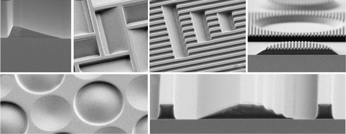
Featured surfaces 3D micro- and nanoscale structures in a thin PMMA film formed by thermally activated selective topography equilibration, which allows sloped, convex and concave profiles to be shaped for applications in optics and fluidics. Such structures can be replicated by NIL but not by photolithography. (Courtesy: Nano Convergence)
Whereas NIL-based semiconductor chip patterning requires a small stamp that is repeatedly imprinted until the entire wafer is fully covered (a so-called step-and-repeat process that demands successive chip levels to be aligned within a few nanometres), new applications such as large-area wire-grid polarizers for displays, high-brightness light-emitting diodes (LEDs), or patterned magnetic media only need single-layer patterning with a stamp that covers the full size of the substrate. For hard-disk applications, for instance, the full surface area of the disk has to be covered with 15nm-wide magnetic data bits arranged in concentric circles – a process that would take several weeks using electron-beam lithography.
Cutting costs
For LED production, which is much simpler than patterned magnetic media, NIL has already been successful in replacing photolithography because it offered lower costs when the industry switched from 100mm to 150mm wafer formats. The sapphire substrates are currently patterned to enable defect-free epitaxial growth of the active gallium-nitride LED layers, but in the future it is likely that photonic-crystal patterns will be employed on the top of the LEDs to enhance light extraction. Resolutions of several hundred nanometres have been demonstrated, but this is expected to decrease as the technique is taken up by other industries. Recently, for instance, the German firm ULM Photonics (which is part of Philips) established NIL as its production method for polarizing gratings on vertically emitting semiconductor lasers.
NIL has thus proved successful in completely different applications from semiconductor manufacturing, where extreme resolution and the overlay of different levels do not play such a big role. Thanks to the range of optical effects possible with diffractive gratings or specific surface textures, numerous further applications seem possible. These include antireflective coatings on screens, solar cells with improved efficiency, “Gecko” surfaces with engineered adhesion, “shark-skin” surfaces that reduce drag in water, and even LEGO bricks with structural rather than pigment-based colouring.
NIL for the future
These applications, along with many bio-applications such as surface patterns for controlling cell growth, seem a world away from the original NIL process. They profit from a toolbox for stamp manufacturing that has been established over the past 20 years, which includes 3D surface patterning and replication by different moulding processes such as injection moulding and roll embossing. This has been complemented by European projects such as NaPa and NaPANIL, which have resulted in a “library of processes” that makes NIL more accessible to researchers and engineers.
Killer applications, such as semiconductor chip manufacturing with highly standardized processes and tools, ensure that NIL will continue to drive key industrial domains. Meanwhile, new applications such as hard disks and LEDs will profit from the broad process methods available, which can be adapted to large areas, non-flat surfaces and functional materials.
After 20 years of development, NIL is now mature and is already used on an industrial scale for LED manufacturing. Future progress will depend on it helping with applications that need simple solutions for large areas to be imprinted quickly, and to do so reliably and with few defects. The next five years will prove not only whether NIL has established itself as a technology driver, but also if it has succeeded in changing our thinking about how technologies are integrated into existing and new process chains.
I am a condensed-matter physicist by training and sometimes I struggle to get excited by the latest breakthrough in particle physics – usually because most don’t seem much like breakthroughs to me. The latest hot paper from physicists working on the Large Hadron Collider (LHC) at CERN is a perfect example of what I am talking about.
Writing in Nature this week, physicists working on the CMS and LHCb experiments at CERN announced the discovery of a rare decay of the strange B-meson, as well as further information regarding an even rarer decay of the B0-meson. In both cases the decays produce two oppositely charged muons. An animation of how the strange B-meson decay is detected by the CMS appears in the video above.
A new method for using light to cool solids has been created by physicists in France and Germany. The technique uses quasiparticles called “polaritons” to remove vibrational heat from a tiny piece of semiconductor, and unlike previous optical cooling schemes it works at very low temperatures. The scheme could provide a new way of cooling very small electronic devices, as well as giving physicists an alternative approach to studying heat transport.
Developed by Maxime Richard of the University of Grenoble and colleagues, the new cooling technique is based on “anti-Stokes fluorescence” (ASF), which has already been used with limited success to cool solids. In the case of a semiconductor, this involves laser light being used to create an electron–hole pair, or “exciton”, in the material, which can then absorb one or more thermal vibrations (phonons). The exciton will go on to decay into a photon that carries with it the thermal energy.
Physicists have been able to use ASF to cool a semiconductor from room temperature to 260 K – a difference of about 30 K. Achieving more cooling power is difficult because defects in the semiconductor cause some excitons to decay and return heat to the material via multiple phonons. Some of the laser light therefore heats the material, rather than cooling it.
Polariton sandwich
The new variant of ASF gets round this problem by not using excitons but polaritons, which form when photons interact strongly with excitons. The technique involves confining the polaritons within a semiconductor microcavity, which is essentially a semiconductor material sandwiched between two semi-transparent mirrors. This confinement imposes a non-zero minimum energy on the polariton, which means that it cannot decay via phonons alone.
Another important benefit of the scheme is that polaritons interact strongly with thermal phonons and polaritons are able to absorb phonons over a wide range of energies. This includes very low energies, which means that the technique should work at very low temperatures.
While the researchers admit that building a practical cooling system based on polaritons would be a technological challenge, they have made preliminary measurements that suggest the technique should work in principle. Their experiment involves firing a laser into the microcavity through one of the mirrors. Polaritons are formed in the semiconductor as the photons bounce back and forth.
Fast and slow cooling
The polariton can then undergo one of two cooling interactions with phonons. “Fast cooling” involves the absorption of one phonon followed by the emission of an ASF photon and is so-called because it happens in about 1 ps. The “slow cooling” interaction takes about 200 ps and begins with absorption of a phonon, then the emission of a lower-energy phonon and finally an ASF photon. Although some heat is returned to the semiconductor during slow cooling, the net cooling effect is actually greater than with fast cooling.
The team confirmed the existence of these processes by detecting the ASF photons that are emitted from the cavity and thus the amount of heat that is being removed from the system. The measurements were obtained over a range of laser intensities and temperatures, allowing the researchers to identify regions in this parameter space where the cooling power is greatest. The results show that big cooling powers can be achieved at temperatures down to at least 4.2 K, which is the lowest tested.
Richard told physicsworld.com that the team is now planning to use the latest nano-fabrication techniques to build a “polariton refrigerator” that measures several tens of microns across and should be able to cool tiny objects. He also points out that “polaritons are a model system of a highly non-equilbrium gas”, and so the team plans to use the system to study how its non-equilibrium properties affect the transport of heat.
I’m sure that many of us, while watching videos of astronauts on board the International Space Station (ISS), floating around with their halo-like hair, have given much thought to how they shower, wash their hair, brush their teeth and, indeed, poop and pee! Well, you can stop stretching your imagination and take a look for yourself – we spotted this story on the Slate website, where you can see the latest videos from the European Space agency, where Italian astronaut Samantha Cristoforetti, who is currently on the ISS, gives us a tour of both the toilet (above) and the “shower” area (below). She even demonstrates exactly how to wash your hair in space – it looks rather fuss-free if you ask me!
A little over 30 years ago, the invention of the scanning tunnelling microscope (STM) revolutionized surface science and helped jumpstart the field of nanoscience. The STM and related tools such as the atomic force microscope allow researchers to quickly visualize individual atoms and molecules. However, they have one key weakness: they can only probe the top surface of an object. Is it possible to overcome this limitation with a microscope that looks below surfaces and directly images molecular structures in 3D at the atomic scale? This question underpins the emerging field of nanoscale magnetic resonance imaging, or nanoMRI – a technique that could represent a major breakthrough in microscopy and have a profound impact on some of the most pressing questions in structural biology.
The current gold standard for solving molecular structures is X-ray crystallography, in which an intense beam of X-rays is diffracted by atoms in a crystalline array of molecules. The diffraction pattern can be mathematically inverted to give the atomic structure of the molecules, unlocking the workings of fundamental biological units such as the ribosome and allowing pharmaceutical companies to develop more targeted drugs. However, X-ray crystallography can be applied only to those molecules that can be purified and crystallized, which represents a small fraction of biologically important structures. Nuclear magnetic resonance (NMR) spectroscopy is an alternative way to solve molecular structures, but it encounters difficulties for molecules above a certain size. Cryo-electron microscopy is also making strides in the pursuit of single-molecule imaging, but as with all forms of electron microscopy, radiation damage is a major issue.
Magnetic resonance imaging (MRI), a well-known technique in the medical arena, suggests an alternative approach. MRI is non-destructive, elementally selective and able to image below a surface in 3D. Like NMR spectroscopy, MRI relies on the detection of the weak magnetism associated with atomic nuclei, typically hydrogen nuclei (protons) in water and organic molecules. In the presence of a magnetic field, these nuclear spins precess at a certain frequency determined by the magnetic moment of the nucleus and the strength of the magnetic field. By imposing a gradient in the magnetic field, the precession frequency becomes spatially dependent, allowing images to be formed by analysing the frequencies of signals detected via an inductive receiver coil.
At first glance, the idea of extending MRI to the nanoscale seems preposterous. After all, nuclear magnetism is a notoriously weak effect because of the tiny value of the nuclear magnetic moment and the disorganized (paramagnetic) nature of the magnetism. For example, a single volume element in a medical MRI image typically requires at least 1018 nuclei to produce a detectable signal, resulting in a resolution in the millimetre to sub-millimetre range. In order to image molecular structure we require a resolution of 1nm or better, necessitating a sensitivity improvement of at least 1016! Clearly great improvements in detection are required.
Feeling the force
The first serious proposal to extend MRI to the nanoscale came in 1991 from medical physicist John Sidles at the University of Washington. In a series of theoretical papers, Sidles outlined a method – now known as magnetic resonance force microscopy (MRFM) – for dramatically improving detection sensitivity based on the measurement of ultra-small magnetic forces. The technique exploits an effect every child learns at school: that two magnets either attract or repel one another depending on their orientation. In MRFM, the two magnets are a nanoscale ferromagnetic tip and the nuclear spins in the sample. By periodically flipping the orientation of nuclear spins in the sample using radio-frequency magnetic fields, the force between the tip and the sample nuclei is made to oscillate. The oscillating force is very weak, typically in the attonewton (10–18N) range, and is detected by the slight vibration of a nanomechanical cantilever.
At the time of Sidles’ proposal, my group at IBM was working on new techniques in force microscopy and we agreed to test the MRFM idea. Since electron spins have a larger magnetic moment than nuclear spins, and thus provide a larger force signal, we decided to focus first on an electron spin-resonance experiment. After modifying one of our existing force-detection set-ups, I placed a microscopic crystal onto a small silicon-nitride cantilever and positioned it close to a small permanent magnet. To my delight, when I then turned on the radio-frequency magnetic field to periodically flip the spins in the sample, I was able to detect tiny oscillations of the cantilever caused by the flipping of the electron spins. Additional demonstration experiments at the micrometre scale followed quickly, including nuclear spin detection. As we continued to miniaturize the experiment, the field gradient from the permanent magnet increased, which allowed us to demonstrate 3D imaging of both electron-spin and nuclear-spin samples.
While micrometre-scale detection was fairly straightforward, extending the technique to the nanometre scale required a more serious effort. The key issue is the extremely small magnitude of the magnetic force generated by nanometre volumes of unpolarized spins, which requires a very small and sensitive cantilever with a low internal friction operating at low temperatures. In work carried out with John Mamin at IBM and students of Tom Kenny at Stanford University, we fabricated 100nm thick, single-crystal silicon cantilevers that enabled us to achieve attonewton force sensitivity when operated at liquid-helium temperatures.
The advent of attonewton force sensing led to several key demonstrations of MRFM, with our group detecting a single electron spin in 2004. A few years later, we achieved an even more significant demonstration: 3D nanoscale MRI of a virus particle with a resolution better than 10nm. Notable progress has also been made at several other institutions. Raffi Budakian and colleagues at the University of Illinois have pioneered the use of semiconductor nanowires for force detection, for instance, while Martino Poggio at the University of Basel has imaged multiple nuclear species within nanowires. At the Ohio State University, Chris Hammel and his students have done extensive work using MRFM to study ferromagnetic resonance in nanoscale magnetic objects, while John Marohn’s group at Cornell University has demonstrated ultrasensitive cantilevers with integrated magnetic tips that produce large field gradients.
Diamond alternative
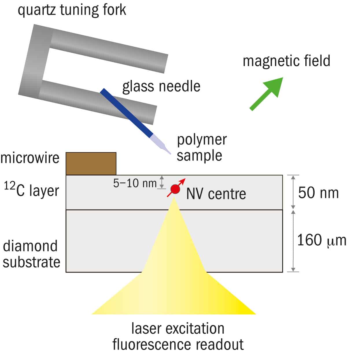
A second detection technique for nanoMRI has recently emerged, based not on cantilevers but on a well-known atomic defect in diamond called a nitrogen vacancy (NV) centre. Here, substituting a nitrogen atom for a carbon atom next to a vacancy in the diamond lattice produces a fortuitous combination of magnetic and optical properties. In particular, individual NV centres can be identified by focusing green laser light onto a diamond crystal and observing a bright, localized red fluorescence.
Diamond detection The experimental configuration used by IBM researchers to demonstrate nanoscale MRI, in which a near-surface nitrogen-vacancy centre in diamond detects a faint magnetic field emanating from the protons in a polymer (PMMA) sample.
Crucially for nanoMRI, the brightness of the NV fluorescence depends on its magnetic spin state, and the precession frequency of the NV spin state can also be measured with great precision. As a result, the NV centre essentially acts as an atomic-size magnetometer with nanotesla sensitivity. The study of individual NV centres was pioneered by Jörg Wrachtrup’s group at the University of Stuttgart in the mid-1990s, and the use of NV centres for nanoMRI detection was proposed in 2008 by Christian Degen, who is now at ETH Zurich.
For nanoMRI applications, where the goal is to detect NMR signals from samples external to the diamond, the NV centre must be located as close to the diamond surface as possible. Near-surface NVs can be formed by ion implantation of nitrogen or by a “delta doping” process during chemical vapour deposition growth of the diamond layer.
One challenge in using near-surface NV centres is the reduction of the spin coherence – the regularity of the NV electron spin precession – because of poorly understood noise sources on the diamond surface. Recent advances in diamond surface preparation now allow NV centres with reasonably good characteristics – namely long coherence times and adequate photostability – to be formed just a few nanometres below the diamond surface.
The first demonstrations of NV-detected NMR from an external sample were achieved in 2012 by the Stuttgart group and, independently, by my group at IBM working in collaboration with David Awschalom, then at the University of California, Santa Barbara. In the Stuttgart work, a sequence of microwave pulses applied to the NV centre enabled the measurement of the oscillating magnetic field that naturally emanates from precessing hydrogen nuclei in an organic sample that was applied to the diamond surface.
In contrast, the IBM approach used a more active manipulation technique whereby the sample’s nuclear spins were flipped using radio-frequency magnetic fields. In both cases, the effect on the NV spin precession is detected via changes in the optical fluorescence of the NV centre. Although no imaging was involved in these initial demonstrations, it was clear from model calculations that the detected signals indeed originated from the hydrogen nuclei within a nanoscale sample volume.
Triple success
Recently these two groups and a third team at Harvard University independently succeeded in extending NV-based NMR detection into the realm of nanoMRI (Nature Nanotechnology10110, 125 and 129). Our group at IBM used a mechanical scanning approach to obtain a 2D hydrogen image of a polymer test sample that was scanned past a single NV centre, demonstrating a resolution of the order of 12nm. The Stuttgart team used a similar approach whereby a patterned fluorocarbon sample was scanned over the NV centre and signals from both hydrogen and flourine-19 nuclei were detected. The third paper, from Ron Walsworth and colleagues at Harvard, used a dense layer of NV centres implanted just below the surface of a diamond substrate and employed a CCD camera to take a wide-field microscope image of NV fluorescence, achieving submicron MRI resolution without the need for mechanical scanning.
These initial demonstrations of NV-detected MRI are just a starting point, and we can expect great improvements in capability as researchers continue to improve the performance of NV-centre signal detection. The signal-to-noise ratio is currently limited by inefficiencies in the detection of the NV fluorescence, for example, but this could be overcome by incorporating recent innovations in diamond optical-waveguide techniques.
Another innovative idea, recently demonstrated by Mikhail Lukin’s group at Harvard, is to use “reporter” electron spins embedded in the sample molecule itself to act as an intermediary between the nuclear spins in the sample and the NV centre. By adding large field gradients to the NV detection system, we should be able to extend the technique to full 3D imaging, although ultimately it might require cryogenic temperatures to achieve the necessary scanning stability and NV coherence time required for a true molecular-structure microscope.
Both MRFM and NV-centre techniques have taken the resolution of MRI well beyond what anyone could have expected just a few years ago. It is clear that nanoMRI is no longer just a dream of a few far-out thinkers. Hopefully, the recent demonstrations will spur even more innovations to push the field forward.


 By James Dacey in Mexico City