

How a decades-old laser technology could boost the future of wind energy

On a coastal plain in Østerild, north Denmark, a gargantuan white structure turns solemnly in the breeze. The latest wind turbine designed by the Danish manufacturer Vestas, the V164, is the biggest yet: at 220 m, it is well over twice the height of the Statue of Liberty. And when it was finally tested in Østerild at the beginning of 2014, it also proved to be the world’s most powerful – capable of generating 8 MW of power, enough to provide electricity for some 7500 homes.

The V164 is a symbol of the wind industry’s recent success. Over the past 14 years, the number of installed turbines across the world has risen dramatically, from an output of just 17 MW in 2000 to nearly 320,000 MW last year – corresponding to about 4% of the world’s total energy demand, according to the Global Wind Energy Council. The boom has been due partly to a surge in the construction of turbines in China, but many smaller countries are also adopting the technology. The UK, for example, generated 10% of its electricity from wind power last year, and it has more offshore wind capacity than the rest of the world combined.

Despite this success, however, the industry has sometimes struggled politically – not least because of a conflict between the cost and location of wind farms. Onshore wind power is relatively cheap: it costs about $87 per megawatt-hour, midway between natural gas ($66/MWh) and coal ($100/MWh), according to a 2013 report by the Energy Information Administration (an agency of the US Department of Energy). Plans for new onshore wind farms often face strong local opposition, however, which is why politicians frequently look offshore for new opportunities. But offshore wind is far more costly: the same 2013 report rates it as more expensive than nearly any other energy technology – renewable or otherwise – at about $222/MWh. The high cost of offshore wind was highlighted in March this year when Scottish and Southern Energy, a UK gas and electric company, announced that it would cut its investment in offshore turbines in order to assure a two-year price freeze for its customers.

The industry’s continued success, therefore, depends on finding ways to cut costs. One avenue that physicists and engineers are currently exploring uses lidar – essentially a laser version of radar – to improve the siting of wind farms and reduce maintenance costs. Lidar systems can measure the pattern and strength of wind at a distance, which gives wind-energy firms a better idea of how windy a certain location will be before they make the large capital investment required for a new wind farm. Better real-time information about how atmospheric conditions are changing could also make it possible to prepare turbines for outbreaks of turbulence, reducing the risk of expensive damage. The hope is that with a little help from light, wind power will become a more cost-effective technology.

New uses for old physics
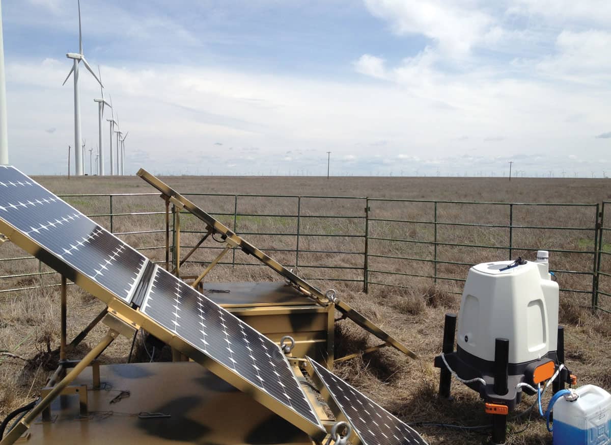
A portable lidar unit

In the simplest form of lidar, laser light (typically infrared) is projected outwards and bounces back off whatever is in its path, including buildings, water, terrain or even – since the wavelength of light is so short – tiny particles in the atmosphere, such as dust and water droplets. The distance to such objects can be calculated from the time it takes for the light to return, or selected in advance by adjusting the laser beam’s focus. Meanwhile, the speed of the objects is calculated from the Doppler shift of the returning light: if the object is receding, the light will be red-shifted, while if it is approaching, the light will be blue-shifted.

In itself, lidar technology is not new. Its development dates back to the late 1960s, when defence experts and meteorologists became interested in using lasers to monitor wind patterns for aircraft landings and measure the distance and size of clouds. Since then, lidar has been used for applications as varied as mapping terrain and crime scenes; making digital models of cities; capturing tiny features of building façades for restoration; checking the speed of motorists; navigating autonomous vehicles; and estimating the concentration of atmospheric pollutants. It has even been used to measure the distance from the Earth to the Moon.

But although lidar is considered a mature technology, many of these well-established applications require lidar units that are far too complex for non-specialists to handle. “You’d need a truck load of PhDs to operate them,” says Mike Harris, chief scientist at ZephIR Lidar, a company based in Ledbury, UK. Another problem is that lidar units tend to be fragile, and are thus unsuitable for use over windy seas or terrain.

The source of both troubles, Harris explains, is that many lidar units have a very small tolerance for optical misalignment. This is especially true of lidars that measure Doppler shift, since they commonly compare the reflected light with a reference beam using interferometry. In this technique, small changes in the wavelength of the reflected light cause it to “beat” with the reference beam, and the timing of these beats reveals the precise extent of the Doppler shift. Since the wavelengths of light are on the order of a micron, the components inside the interferometer must be aligned to within a fraction of a micron in order to give an accurate measurement.

A solution to these problems began arriving in the 1990s, with the widespread adoption of optical fibres by the telecommunications industry. Suddenly, optics became more like electronics: laser light could be routed around enclosures compactly and with high precision, using the optical fibres like wires. And, crucially, fibre optics could suffer exterior movement without having to be re-aligned. “The requirements of the wind industry are pretty stringent,” says Harris. “You’ve got to sit the piece of kit out on the hillside with no maintenance for months on end. And you’ve got to get it there, so it’s got to be light.” Today, says Harris, the performance of lidars is not in question, although further improvements in their cost and reliability might make it more practical to mount them on large numbers of turbines.

Finding sites

Past efforts to reduce the cost of wind power have often focused on turbine technology. As a result, modern wind turbines have become incredibly efficient, capturing nearly 60% of the wind’s kinetic energy – close to the theoretical maximum as calculated in 1919 by the German physicist Albert Betz. Further cost reductions will require a different approach, and lidar technology could make a contribution in several ways.

One of these concerns the siting of wind farms – what the industry terms “resource assessment”. Evaluating a site’s suitability for a wind farm is a major expense for energy companies, requiring wind measurements at multiple points over an extended period, typically one and a half years. Only with such exhaustive measurements – supported by comparisons with historical meteorological data to check there are no anomalies – can a company persuade a bank to lend the initial capital. “It’s no good just putting a wet finger in the air and saying, ‘Yes, that’s windy enough’,” says Harris.

In the past, energy companies have performed such measurements with meteorological masts, commonly known as “met masts”. These masts support anemometers to measure wind speed directly, and must be built into the existing terrain on strong foundations. This doesn’t come cheap: a single offshore met mast, sunk into the seabed, costs around £15m. Performing siting measurements with lidar is inexpensive by comparison. ZephIR’s floating lidar units, for example, cost as little as £500,000 each and have the added benefit of being reusable, so they can be moved around a site or even taken from one site to another. The benefits of lidar for resource assessment were quantified earlier this year by the international renewable-energy consultancy Ecofys, which estimated that using lidar could lead to a total return on investment of as much as 14.5%, as opposed to 11.8% with met masts.

The other main application of lidar in the wind industry involves making measurements of atmospheric conditions up-wind from operating turbines and using these data to prepare for turbulence. If a turbine is subjected to turbulence it is unprepared for, its blades can suffer extremely high loads that, while not necessarily leading to sudden failure, can cause accumulated fatigue that costs millions to repair. “It’s a bit like driving over a pothole,” says Harris. “It knackers your suspension.” In 2008 a wind turbine near Hornslet in Denmark exploded, apparently because costly maintenance had not been carried out on its gearbox.

One idea is to build a lidar unit into the hub at the centre of a wind turbine, where it can analyse the pattern of incoming wind. If turbulence is known to be imminent, the pitch of the turbine blades can be altered so that they cause less wind resistance and, as a result, suffer a reduced load. This will lower the maintenance required for existing turbines, but Harris believes it could also enable turbines to be manufactured more cheaply, because they would not have to be “over-engineered” to prevent failures such as the one near Hornslet.

Making a contribution
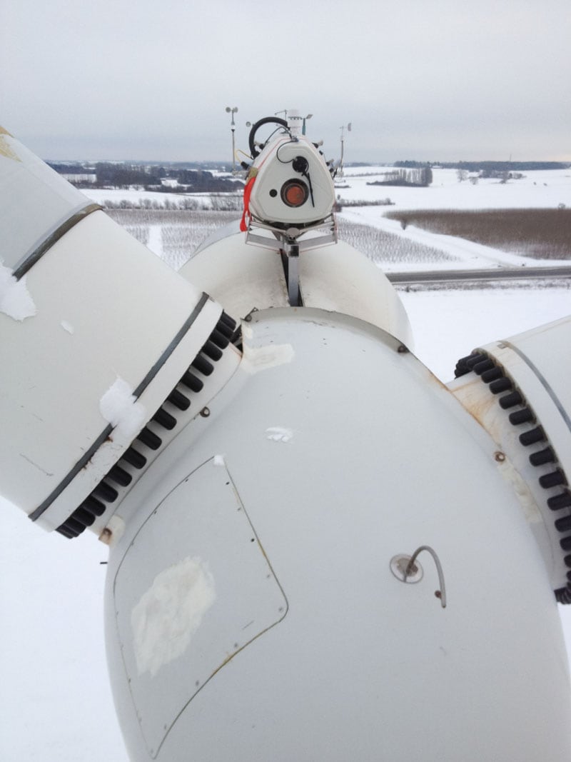
A lidar unit mounted on a turbine

The idea of using lidar to prepare turbines for turbulence is attractive, but it is not the only solution. Some engineers are experimenting with integrated load sensors that quickly detect the onset of turbulence and adjust the blade pitch accordingly. Furthermore, some turbines are being developed with systems that control the pitch of individual blades, meaning that the response to turbulence could vary from blade to blade. This level of control is important because eddies can be very localized, and, under these circumstances, “having a lidar to look upstream is probably not going to help you”, says David Infield, a mathematician and expert in wind power at the University of Strathclyde, UK.

Infield is also unconvinced that lidar units offer a comprehensive alternative to met masts. In some cases, he argues, “there’s going to be issues over whether a company would want to leave an expensive lidar unit on site for a year or more”. Nonetheless, he believes lidar technology has some attractions for the wind industry. “The benefit of lidar is that it can give a much more complete description of the wind’s shear profile, and, especially on shore, you can deploy [lidar units] relatively straightforwardly,” he says. “At the moment, my understanding is that [energy companies] are usually using it to complement long-term measurements from masts.”

Lidar could also have uses for wind-power research. At Strathclyde, one of the world’s leading centres for such studies, scientists have been using lidar to understand the 3D pattern of turbine wakes, and how they affect the performance of other, downwind turbines, Infield says. Meanwhile, researchers at ZephIR are trying to attach lidar units to turbine blades, to understand how they are interacting with the wind in real time. Such investigations could ultimately lead to better-performing and more cost-effective wind farms, although Harris warns that there is a lot of uncertainty in the accuracy of lidar data, depending on the frequency of scanning and other details.

But regardless of where lidar is ultimately applied in the wind industry, it seems destined to lead to improvements. The pioneering work of ZephIR has already been honoured, with the UK secretary of state for business, Vince Cable, presenting the company last year with an Innovation Award from the Institute of Physics (IOP), which publishes Physics World. “ZephIR has addressed an ongoing problem for firms trying to bring affordable and reliable wind power to the grid,” said the IOP president Sir Peter Knight. “It is highly deserving of this award.”

Harris, however, prefers to remain modest about the potential of his company’s technology. “It’s certainly got a contribution to make,” he says. “Not on its own is it going to drag the wind industry from any current perceived problems – but it’s got a contribution to make.”

Swedish nano centre eyes up clean energy

What is the nmC in a nutshell?

The Nanometer Structure Consortium (nmC) engages more than 200 scientists from three faculties to work on interdisciplinary nanoscience. Our scientific focus is on the materials science, physics, chemistry and safety of designed functional nanostructures, and their use in a wide range of applications including sustainable energy, optoelectronics and the life sciences. We have a particularly strong position internationally in semiconductor nanowires based on groups III and V of the periodic table.

Were you one of the first nanotechnology centres to be created?

The centre was founded in 1988 by Lars Samuelson, who led it until last year, with inspiration from the University of Glasgow and IBM Research in Zürich. In comparison, the US National Nanotechnology Initiative came along about 10 years later, so it is true that we were one of the first centres.

How has the group’s focus changed?

Throughout the past 25 years, the nmC has consistently emphasized materials science and quantum physics as its core competences. In the first decade, the scientific focus was on self-organized quantum dots and 2D electron gases. Then in around 2000 a conscious decision was made to pursue group III-V semiconductor nanowires, initially with expected applications in nanophysics research but also in electronics and optoelectronics. Over the past five years we have expanded our range of applications to include sustainable energy, neuroscience and other biomedical research. We also added a large nano-safety group that is working to understand the effects of nanowires and other nanoparticles on cells, organisms and the environment to ensure that we will be able to address any safety concerns early.

How can nanotechnology deliver cleaner energy?

Nanotechnology is about controlling and applying the new phenomena that occur at the nanoscale. In the case of nanowires, there are several such phenomena that are important for energy applications. First, they can be grown in ordered arrays, which allows them to act as photonic systems for more effective light harvesting in nanowire-based solar cells. Second, the small diameter of nanowires lets one combine different materials, even with drastically different lattice constants, into radial or axial heterostructures that may be used to create cheaper multi-junction solar cells and LEDs with higher efficiency and better colour rendering. Third, quantum-confinement effects can be used to tune the energy of photons emitted by nanowire LEDs and to enhance their thermoelectric power output. Finally, the interfaces formed in nanoscale materials can be used to control heat flow in thermal management or to suppress parasitic heat flow in thermoelectrics.

How will your PhD4Energy project help bring this about?

The project is part of the European Union’s Marie Curie Innovative Doctoral Programme and will run for four years. Worth 73.2m (about $4.46m), it will place 12 PhD students at the nmC to work on nanostructures for clean-energy applications. PhD4Energy is important for us because it adds critical mass and engages all parts of our very broad consortium of research groups, helping us to maintain a joint focus. The project ranges from applied research, such as nanowire-based solar cells, LEDs and thermoelectrics, to fundamental research on novel paradigms for nanoscale energy conversion, such as artificial molecular motors. Studies on the safety of nanowires are an integral part of the project.

What impact do you expect the project to have?

Scientific goals include studying cost-competitive, nanowire-based multi-junction solar cells, high-efficiency solid-state lighting and developing methods to increase the power output from nanoscale thermoelectrics. Each PhD student will also take up an internship with one of the eight firms that are associate partners of the project. In addition, we will collaborate closely with spin-off companies that commercialize nanowire-based devices from our environment. Specifically for LEDs, we have already created Glo and for solar cells we have Sol Voltaics.

What are the group’s long-term plans in energy research?

Using this project as a platform, we hope to build a lasting internship programme with many more participating Swedish and international companies. Scientifically, a long-term aim is to develop and then realize entirely new device paradigms that use nanophysics for efficient energy use or for energy conversion.

Has too much hope been placed on nanotechnology to solve society’s problems?

Our group has deliberately stayed away from unrealistic science-fiction dreams of what “nano” could bring – we won’t see true nanobots, for example. But the emerging approaches for drug delivery, diagnostics and therapy achieve things that were hard to imagine 25 years ago. Also, the way that information technology has changed our society has only been possible because of nanotechnology. So, I would say that nanotechnology is living up to expectations and will probably even exceed them for some time to come. The important thing is to keep investing in fundamental science along with applied science because real breakthroughs require the combination of both.

Nanocoatings keep water at bay

Of all the reasons given to mobile-phone manufacturers for broken handsets, top of the list are rainwater, toilets and washing machines. But perhaps not for much longer, thanks to nanocoatings that cause water droplets to simply roll off a surface as they might a plant leaf. UK firm P2i has recently installed numerous plasma-deposition machines in Motorola production lines to coat handsets with a tough, splash-proof polymer layer. More than 60 million electronic devices have already been treated using the technique and the company is about to release a “dunkable” coating that will keep a device functioning after being submerged for up to 30 minutes.

P2i, which was spun out from the UK’s Ministry of Defence a decade ago, developed a pulsed-plasma deposition process that applies an ultrathin polymer coating onto the internal and external surfaces of mobile devices. The invisible, Teflon-like layer dramatically lowers the surface energy of a material, which makes the water bead and allows “pretty much anything” to be coated with it in a matter of seconds, according to the firm’s chief technology officer Stephen Coulson. “It can be applied to any material, such as clothing, shoes and cardboard,” he says. “Such coatings also have low liquid retention, so you get less cross contamination between surfaces, and they could also be used for filtration and even to make fire-retardant surfaces.”

Non-wetting technology first garnered attention in the 1930s and 1940s when scientists started to understand how nature does it. Studies of duck feathers, for instance, revealed the crucial role of trapped air in keeping water off but it also became clear that the microscopic structure of a surface was vital too because it controls the angle that a droplet creates with it. A droplet landing on a textured surface, such as the lotus leaf, has a contact angle of up to 170°, making it almost spherical and classifying the leaf as “superhydrophobic”.

Numerous sprays and products have been engineered to mimic the lotus leaf’s behaviour, but our ability to characterize and fabricate structures at the micro- and nanoscale has led to an explosion in this subject over the last 20 years, says Kripa Varanasi of the Massachusetts Institute of Technology (MIT) in the US. Texture amplifies the intrinsic wetting properties of a material, allowing researchers to design even more extreme hydrophobic coatings, including those engineered to deal not just with static droplets, but impacting ones.

Last year, Varanasi and co-workers set a new record for superhydrophobicity by structuring materials including silicon, copper and aluminium with ridges that make droplets rebound more easily when they strike the surface. The patterns, which are similar to those found on butterfly wings and nasturtium leaves, minimize the contact time between the drop and the surface, and make the material 40% more hydrophobic than previously thought possible (Nature 503 385). The principle could have important industrial applications in enhanced waterproofing, says Varanasi, for example to reduce the formation of ice on power lines and aero-engine turbines.

Tough challenge

The main hurdle in getting such coatings widely adopted is to ensure they are durable. The plasma technology used by P2i to coat mobile devices bonds the coating covalently to a material surface, which is hardy enough to survive the rigours of everyday use. But hydrophobic coatings that can withstand the much harsher environment of a steam turbine could deliver massive energy savings because up to 20% of losses in such machines come from tiny droplets settling on the blades and forming a thin film, explains Varanasi. His group is currently investigating the use of special ceramics and other covalently bonded coatings for commercialization in the energy industry, and is also targeting clathrate-proof surfaces for the oil and gas sector.

In 2012 the MIT group founded “Liquiglide” to commercialize coatings that allow 100% dispensing from containers by replacing the air pockets between structured surfaces with a lubricant. The technology, which is due to hit the market next year, generates a very thin Van der Waals film between a product and the substrate allowing consumers to extract every drop of ketchup or toothpaste from a container. “The beauty with this is that you don’t have to rely on polymers, you just need a lubricant that doesn’t dissolve in your product,” Varanasi told Physics World.

According to Coulson, who was a PhD student at Durham University in the UK when he invented P2i’s polymer-coating technology to provide soldiers with protective clothing, we are on the brink of a smart-coating revolution. Today, P2i has 62 patent families and is focusing on making electronic boards not only hydrophobic but electrically isolating, as well as developing protecting filters that repel water while allowing air to flow. “There are lots of liquid-based solutions out there, but most tend to shrink-wrap a product rather than bind to it,” says Coulson. “The key is how you apply coatings and make the process cost-effective.”

2D materials: graphene and beyond

The unique electronic, optical, chemical and mechanical properties of 2D materials are creating a flurry of interest in laboratories around the world. Made up of individual atomic planes weakly held together by Van der Waals forces, these apparently simple systems behave very differently to their 3D counterparts and are therefore seen as a promising route for new electronic and other devices. The most widely studied 2D crystal is graphene: a planar sheet of carbon atoms arranged in a honeycomb lattice that is thinner and stronger than any other known material.

Since it was first isolated in 2004, graphene has continued to surprise. Some researchers believe that it might even become as important as silicon for the electronics industry. This is because electrons whizz through its 2D lattice at extremely high speeds, behaving like “Dirac” particles with no rest mass, which leads to extremely high conductivity. Graphene also shows great promise for photonics applications because it has an ideal internal quantum efficiency: almost every photon absorbed generates an electron–hole pair that could, in principle, be converted into electric current. And thanks to its Dirac electrons, graphene can also absorb light of any colour and has an extremely fast response, which could lead to much quicker optoelectronics devices for telecommunications.

However, graphene’s extreme conductivity is also a problem because the material remains conducting even when the power is switched off – wasting energy and preventing graphene components from being packed into computer chips as silicon components are today. There are other reasons why all is not plain sailing with this 2D wonder material. Although graphene is a semi-metal or “zero-gap” semiconductor, it is unlike familiar semiconductors such as silicon because it does not have an energy gap between its valence and conduction bands. Such a band gap allows a semiconductor to switch the flow of electrons on and off, which is the principle by which transistors operate. Researchers have proposed various schemes to overcome this problem, for example cutting graphene into nanoscale ribbons or chemically modifying the material to make it properly semiconducting, but such approaches damage the material and spoil its high electron mobility.

These drawbacks have turned researchers’ attention to 2D materials that naturally possess a band gap, such as transition-metal dichalcogenides (TMDCs), hexagonal boron nitride and layered oxides. These monolayer materials might even be combined with graphene to make novel hybrid heterostructures that have exceptional electronic and mechanical properties. “This new class of materials promises all: insulators, metals, semiconductors and superconductors,” says Sefaatin Tongay of Arizona State University in the US.

Semiconductor promise

TMDCs consist of a layer of transition-metal atoms sandwiched between two layers of chalcogen atoms, such as sulphur, selenium or tellurium, and they can be made using similar methods employed to obtain graphene. In bulk form, TMDCs are indirect band-gap semiconductors, but when scaled down to monolayers, the strong coupling between the neighbouring layers turns them into direct band-gap semiconductors. The material is therefore very efficient at absorbing and emitting light, and because TMDCs can be placed on a variety of substrates, they are ideal for optoelectronic devices such as LEDs and solar cells.

One much-studied TMDC, which is made from molybdenum and sulphur (MoS2), shows particular promise. But others discovered in the past few years include MoSe2, NbS2, ReSe2 and WSe2 (see table below). These materials could find similar applications as proposed for graphene or, if combined with graphene’s unique electronic and mechanical properties, could be used to make superior nanoelectronic circuits.

Earlier this year, however, Tongay and colleagues discovered a new 2D material called rhenium disulphide. Despite officially being a member of the semiconducting layered TMDC family, the material behaves as though it is a pure monolayer. Unlike other 2D materials though, it does not undergo an indirect-to-direct band-gap transition when scaled down to monolayers. The system therefore provides researchers with a 3D crystal in which they can study 2D phenomena without the difficulty of preparing large and high-quality monolayers.

Perhaps the next-best material to graphene in terms of mechanical and thermal properties is hexagonal boron nitride

Perhaps the next-best material to graphene in terms of mechanical and thermal properties is hexagonal boron nitride (hBN). Also known as “white graphene”, hBN is an ideal substrate for graphene because the two materials have very similar lattice constants. Unlike graphene, hBN is an insulator with a very large energy band gap, which means that monolayers of hBN integrated with graphene can be used as gate dielectrics and tunnel barriers with very few defects.

Indeed, hBN has particularly strong phonon resonances in the technologically important infrared band, which some physicists believe could be used to process information in nanodevices. “Flexible nanoelectronics could be the main application for the portfolio of 2D materials where graphene, TMDCs and hBN might be combined to make high-performance ultra-flexible transparent transistors on plastics and soft substrates,” says Deji Akinwande of the University of Texas at Austin.

Graphene derivative

Since graphene first rocked the materials world a decade ago, researchers have been exploring derivatives such as fluorographene, which is a wide-gap insulator made by fluorinating graphene. Similarly, the large band gaps in “graphane” and “graphone” (hydrogenated and semi-hydrogenated versions of graphene, respectively) could be used to make transistors with a large on–off current ratio, although researchers first need to find a way to prevent these materials from gradually losing their hydrogen atoms. Researchers are also exploring “graphynes”: 2D carbon allotropes built from double- and triply-bonded carbon atoms instead of just double bonds. These materials naturally contain conducting charge carriers and therefore could be made into semiconductors without the need for external doping.

According to some researchers, one of the most promising graphene-based derivatives is graphene oxide. This material is just like ordinary graphene but is covered with molecules such as hydroxyl groups or oxygen, which remove electronic states and turn the graphene into an insulator. Sheets of graphene oxide can easily be stacked on top of each other to form extremely thin but mechanically strong membranes, which could serve as molecular sieves. In addition to applications in water filtration and desalination, such systems might also be used for hydrogen storage, polymer solar cells, and flexible colour displays and smart textiles.

It is not yet clear whether graphene will live up to its promise and “win out” over other 2D materials, nor when the 2D-materials revolution will really start to affect our lives. According to Tongay, it is likely that there will be many winners in the race and that more competitors will appear relatively soon, such as phosphorene and silicene. “Graphene kick-started the 2D materials field and will remain an integral member of the 2D family, but the other 2D materials will bring new functionalities,” he says. “The 2D-materials revolution is here and I very much hope to see these materials integrated into our daily lives in different forms, from flexible electronics and solar cells to applications that we have not even dreamed of yet.”

The most promising 2D materials

Graphene family

Graphene – Extremely high conductivity and mechanical strength but no band gap in pristine state

Graphene oxide – Promising for molecular sieves, hydrogen storage and polymer solar cells

Graphane and graphone – Large on–off current ratio and large band gap but gradually lose hydrogen

Graphyne – Naturally contains conducting charge carriers

hBN (white graphene) – Good mechanical and thermal properties; an insulator and exceptional substrate for graphene

Fluro- and chlorographene – Often called the 2D version of Teflon, demonstrating insulating  properties

BCN – Electronic properties ranging from insulating to semi-metallic

2D dichalcogenides

MoS2, WS2, MoSe2, WSe2 – Good at absorbing/emitting light and high charge mobility

Semiconducting dichalcogenides (e.g. MoTe2, WTe2, ZrS2, ZrSe2, ReS2) – Good for low-friction applications, such as lubricants

Metallic dichalcogenides (e.g. NbSe2, NbS2, TaS2, TiS2, NiSe2) – Some become superconductors below a certain temperature

Layered semiconductors (e.g. GaSe, GaTe, InSe, Bi2Se3) – Can be exfoliated onto a number of different substrates

2D oxides

Micas, BSCCO – Wide band gap; potential for all-oxide electronics, thermoelectrics and fuel cells

Layered copper oxides – Could become high-temperature superconductors when charge carriers are added to the layers

MoO3, WO3, SnS2, SnSe2, SnTe2 – Might be good for doping carbon nanotubes

TiO2, MnO2, V2O5, TaO3, RuO2 – Wide-ranging electronic, chemical and mechanical properties; has potential for thermoelectrics

Hydroxides (e.g. Ni(OH)2, Eu(OH)2) – Strong redox properties

Perovskite-type (e.g. LaNb2O7, Bi4Ti3O12, Ca2Ta2TiO10) – Good substrates for growing cuprates, colossal magnetoresistive manganites and multiferroics

Others

Silicene – Unstable as free-standing sheet

Phosphorene – Natural semiconductor but is difficult to produce in larger sheets

Germene – Natural semiconductor but hard to grow and environmental stability is unknown

(Courtesy: Adapted from A K Geim and I V Grigorieva Nature 499 419)

How to achieve a scientific ‘Arab spring’

In the UK we often grumble when funding agencies request information about how blue-sky research might have an impact or lead to some application or societal benefit. Spare a thought then for the state, and status, of science in the Arab world. The faltering Arab Spring – a wave of protests that began in December 2010 and has since swept through the Arab world – has shown the hunger among many of the 370 million people spread across the Middle East and North Africa for societal change.

But while the traditional powerhouses of the region – Egypt, Iraq and Syria – grapple with more immediate political crises, others such as the oil-rich Gulf States, like Saudi Arabia, are tentatively attempting a cultural renaissance. As with many nations in the developing world, Arab leaders understand that to get the most out of their natural resources, they need to invest in science.

However, what we have yet to see in the region is a scientific Arab Spring – a different sort of awakening that will transform attitudes towards the value of science and scientific research. Yes, government funding for science and education has grown sharply in recent years in many of these countries, but most Arabs are still disengaged from science and see it as a secular, even atheist, Western construct. Most have forgotten the many wonderful contributions – from astronomy to medicine and philosophy – that were made by Arab and Persian scholars during the height of the “golden age” of science that began in the first half of the ninth century and continued for several hundred years.

This was an age epitomized by a spirit of rational enquiry at a time when most of Europe was stuck in the Dark Ages. But this freethinking spirit gradually went into decline in the Middle Ages. Those bygone days are now long forgotten, as, sadly, is the culture of freedom of thought and a curiosity-driven quest for knowledge that so epitomized that period.

Developing scientific research

The most obvious effect of this malaise is the poor quality of academic research in many Arab universities. I sometimes get to review papers submitted to physics journals and on the whole – possibly due to lack of resources and infrastructure – the quality is not like those from the Western world. So should we be trying to encourage them by allowing this work to be published? No, there has to be a level playing field and quality threshold for research publications in the top journals.

An example of where there is a serious attempt to boost the quality of research in the Arab world is the fascinating story of the co-educational King Abdullah University of Science and Technology (KAUST), built on a brand new campus in the desert near Jeddah in Saudi Arabia (see November 2009 pp12–13). This vast new research institution has the third largest endowment of any university in the world after Harvard and Yale.

But it is not simply a matter of throwing money at the problem. Even more important is having the political will to ensure real freedom of thinking. To compete globally requires more than just the latest equipment. The whole infrastructure needs to be addressed – from laboratory technicians who understand how to use and maintain equipment to the exercise of real intellectual freedom on the part of the scientists who must have access to the best books and the latest research journals.

There also needs to be far better quality assurance within universities as well as higher levels of motivation and incentives and better salaries to stop the current brain drain of so many of the brightest minds. Currently, more than half of all Arab students who study abroad do not return home, and one can understand why. Even KAUST has been criticized for not educating enough local students, favouring those from overseas instead.

Finding the right balance

Despite a sharp increase in funding, there remains an overwhelming emphasis on applied research, innovation and technology in areas such as water desalination, energy and agriculture, although we are beginning to see a real shift towards investing in areas like biotechnology and nanotechnology. Even at KAUST, research is focused on supporting Saudi Arabia’s post-oil future in key areas such as exploiting solar energy and developing crops that can survive the country’s hot, dry climate. It is inevitable that such areas will remain a priority in that part of the world, but the right balance between pure and applied research has yet to be found.

If the Arab world hopes to develop a more enlightened culture of scientific research, it cannot afford to ignore curiosity-driven basic research in favour of applied research. Many have questioned whether properly funding blue-sky research in areas such as particle physics or astronomy is a luxury that can be put to one side. But while the standard case for basic research – that it leads to unexpected applications further down the line – always needs to be made, the real reason it is required is that basic research encourages the freedom of thought that is so lacking in the Arab region at the moment.

Indeed, KAUST is an isolated bubble within a still conservative society. It is no good having such research institutions for the select few if there is no interaction with the wider community. One way of nurturing trust in science is by engaging with the general population through science festivals and other forms of public dialogue, which is only slowly beginning to take off in the Arab world. There have been successful festivals run in cities such as Cairo, Doha, Abu Dhabi and Dubai that have been greeted with remarkable enthusiasm and large numbers of attendees. But unlike political reform, which can happen remarkably quickly, I believe that when it comes to science and research, ingrained negative attitudes will take longer to change, but I remain ever-optimistic.

Dwarf planet could illuminate the dark sector

A dwarf-planet candidate called UX25 and its tiny satellite could provide the first evidence of a new cosmological model that includes antigravity, say Alberto Vecchiato and Mario Gai of the Astrophysical Observatory of Turin in Italy. The model dispenses with concepts such as dark matter, dark energy and cosmic inflation, and the astronomers say that it could be tested by observing the motion of the two objects as they move through the outer solar system.

In 1915 Albert Einstein’s fledgling general theory of relativity received a major credibility boost when it was used to explain a discrepancy in Mercury’s orbit that could not be accounted for by Newtonian physics alone. Now, nearly a century later, Vecchiato and Gai have calculated that UX25 and its tiny satellite – which orbit the Sun in the Kuiper belt beyond Neptune – could be used as a “natural laboratory” to test an ambitious new model of the universe.

Gravitational charges

Developed by CERN physicist Dragan Hajdukovic, the model is based upon the concept that empty space – also known as the quantum vacuum – is not really empty at all. Instead, it consists of “virtual” matter and antimatter particles that constantly blink in and out of existence. Hajdukovic’s idea is that these particles have opposing gravitational charges, similar to positive and negative electrical charges. He further predicts that in the presence of a gravitational field, virtual particles in the quantum vacuum will generate a secondary gravitational field that has an amplifying effect. The end result is that galaxies and other objects will appear to have stronger gravitational fields than would be predicted by the mass of their stars alone – a discrepancy that most astronomers explain by invoking the hypothetical and mysterious substance known as dark matter.

In Hajdukovic’s new model of the universe, there is also no need for dark energy, the enigmatic force that scientists think is causing the universe to expand at an accelerated rate. The idea is that if virtual particles have gravitational charges, then space–time itself can exert a kind of pressure that causes objects to repel each other. His theory would also negate the need for cosmic inflation, a theorized rapid swelling of the early universe when space–time itself expanded faster than the speed of light. “My theory provides encouraging initial answers to many different fundamental questions in physics,” says Hajdukovic.

Distant elliptical orbits

Hajdukovic has previously suggested that his theory could be tested if a minor planet with a small satellite that has an elliptical orbit can be found. The system would need to be located far from the Sun and other massive bodies.

Now, Vecchiato and Gai suggest that Hajdukovic’s model can be tested by using existing ground and space telescopes to observe the UX25 system – which is about 43 times farther from the Sun than is the Earth. “The properties of quantum vacuums described in Hajdukovic’s theory would apply an additional [gravitational] force on UX25, perturbing the orbit of the system,” Vecchiato explained to physicsworld.com.

Wobbling moon

Hajdukovic’s model predicts that the wobble, or “precession rate”, of UX25’s tiny moon around the dwarf planet should be larger than is predicted by classical physics. Where Newtonian physics predicts a precession rate of 0.0064 arc seconds – too small to be observed with current methods – Hajdukovic’s theory predicts that the rate should be 0.23 arc seconds per period – just enough to be detectable by NASA’s Hubble Space Telescope and the soon-to-be-launched James Webb Space Telescope.

According to Vecchiato and Gai, a large ground-based telescope such as the Very Large Telescope might also be able to make the necessary observations of UX25.

Evidence for Hajdukovic’s theory would result in a dramatic change in perspective for physicists, says Gai. “Most scientists today think quantum physics is mainly restrained to the microscopic world…In this case, the natural microscopic behaviour of empty space would result in a cumulative, long-range effect acting up to cosmic scales.”

The proposal appears on the arXiv preprint server.

Nanoethical concerns

A colleague at Stony Brook who teaches an online engineering course recently asked me to help students acquire what the syllabus calls “an understanding of professional and ethical responsibility”. Deciding to use nanotechnology as a case study, I created a video about engineering ethics, got the students to read about nanotechnology and then asked them to write a piece on an issue involving “nanoethics”.

Science and engineering students, I have found, generally regard ethics training as a distraction. If they must have it, they want brief, clear instructions on how to identify and solve ethical problems. Unfortunately, ethics doesn’t lend itself to that. Instead, it involves the murkier process of learning how to become sensitive to aspects of a situation that you tend to neglect either because they make you uncomfortable or because you just don’t see them.

The three Is

More specifically, science and engineering students tend to find ethics discussions ineffectual, impossible and intrusive – reasons that I think of as the “three Is”. Ineffectual, because the students see themselves as working on something whose applications – where the ethics is – are somebody else’s business. Impossible, because how can you expect to envision consequences of a new discovery or technology when it doesn’t even exist yet? Intrusive, because students can tend to think that ethical inquiry involves scientifically illiterate outsiders trying to set limits on research when scientists should be free to explore where research takes them.

To set the stage, I had the students read an article from 2005 by the science historian W Patrick McCray entitled “Will small be beautiful? Making policies for our nanotech future” (History and Technology 21 177). This article discusses the creation of the US National Nanotechnology Initiative (NNI) in 2000. McCray begins by quoting a senior adviser at the US National Science Foundation to the effect that the NNI brought about a “phase transition” so that “what had once been perceived as blue sky research…was now being seen as the key technology of the 21st century”.

McCray then discusses the rhetoric used to marshal public and congressional support for this phase transition. The Nobel prize-winning physicist Horst Störmer, for instance, promised that nanotechnology would provide the tools “to play with the ultimate toy box of nature”, noting that “the possibilities to create new things appear endless”. Other scientists argued that nanotechnology could “change the nature of almost every human-made object” and “alter our comprehension of nature and life” – thereby influencing “societal and international relations” and giving rise to a new world called the “nanocosm”.

The nanocosm was promoted with utopian visions that promised industrial competitiveness, medical breakthroughs and even immortality. Some people did make dystopian suggestions of dangers to human health and security – warning of the possibility of disasters that would turn ecosystems into “grey goo” – but the utopian rhetoric was instrumental in creating the excitement that led to the NNI.

McCray’s article makes it easy to counter the first two of the three Is. First, he makes clear that nanotechnology – like much science – intertwines scientific and visionary aspects, both for scientists who do it and for governments that fund it. The potential applications of nanotechnology are usually quite obvious, which is why discussing nano-ethics is in no way an ineffectual exercise. Indeed, nanotechnology perfectly illustrates the “linear-model” fallacy referred to by science-policy analysts, which is that science always begins in the lab detached from a social context and only then do people think about applications. As for the idea that ethics discussions are impossible, the likelihood of specific transformative social impacts was clear to nanotechnology’s researchers and funders from the start, meaning that there are plenty of practical examples to pick from.

The third I – the assumption that ethical inquiry is intrusive to research – is harder to dispel. It springs from the misconception that ethics consists of rules that ethicists dream up. But ethics actually springs from values internal to the everyday practice of science and engineering, such as a desire for openness and avoiding harm. Ethical conflicts arise from clashes between those internal values and the desire of individuals or groups to advance their self-interest. Ethicists do not invent those values, but clarify why they may be compromised and how to head off temptations to do so.

I found that using nanotechnology to teach ethics has limits. For one thing, it creates the illusion that nanotechnology involves a special kind of ethics rather than being a new context for familiar ethical issues, an illusion that has been promoted by numerous books and websites on nanoethics. But as Paul Litton, a professor at the University of Missouri law school, notes in an essay entitled “‘Nanoethics’? What’s new?” (Hastings Center Report 37 22), “None of the ethical concerns associated with nanotechnology is unprecedented and none raises novel ethical issues or demands new ethical principles.” What nanotechnology does, Litton writes, is give us new contexts in which to weigh and balance reasons related to our long-held values: “autonomy, beneficence, fairness, efficiency and environmental preservation”.

The critical point

One student told me that he found the entire exercise frustrating. “I prefer calculus,” he wrote, for “there is always a right and a wrong answer.” People who go into science and engineering, after all, are drawn to problems with exact answers, which ethics does not have. Still, he admitted to being excited enough about nanotechnology to read about its ethical issues.

That illustrated the upside of using nanotechnology to teach ethics. Teaching ethics to students in the middle of a science and engineering class requires delivering a jolt of excitement and the sense of something novel – and discussing nanotechnology delivered. It may pose the same old issues, but served to consolidate their interest long enough to get students to make the phase transition needed to follow through on the readings.

  • The latest Physics World Focus on Nanotechnology is now out in print and digital formats

Relaxation and repulsion helps viruses pack DNA

The molecular motor that folds and packs DNA into a virus is at its most efficient when the DNA shows some self-repulsion. That is the surprising finding of researchers based in the US – it was previously thought that such repulsion would act as an obstacle in the packing process. The team also found that pausing the motor and allowing it to relax increased the rate of the whole packaging process. In addition to providing new insights into how viruses function, the work could benefit biotechnologies that enclose long polymers into nanoscale devices.

After invading its host cell, a virus reprogrammes the cell’s nucleus to duplicate it. As it replicates, a strand of DNA is pulled from an infected host cell and squeezed into a protein shell – known as a prohead – which then carries the DNA to infect other cells. In some species, the prohead is produced first, leaving only a small hole at one end through which a powerful molecular motor pushes the DNA in and then packs it at very high densities. The motor has to overcome three forces: the electrostatic self-resistance that comes into play because DNA is negatively charged; the mechanical resistance of DNA to bending; and the entropic resistance of DNA to be crowded on itself.

Increasing attraction

The DNA could, however, be made attractive – a cell containing positive ions (notably a polyamine called spermidine3+) could stick to the DNA and partially screen the repulsion or even create attractive forces at high concentrations. In the past, certain computational models suggested such attraction might help the packing process. But according to biophysicist Douglas Smith of the University of California, San Diego, who led the new research, the earlier models had assumed the DNA was able to continuously relax to the lowest energy state as it was packaged, and this would reduce resistance.

To test this, Smith and colleagues manoeuvred two microspheres near to each other using optical tweezers, attaching viral DNA to the first and the molecular motor to the second. Occasionally, the molecular motor managed to grab hold of the DNA and pull it from one microsphere to the second in a process that Smith compares to fishing. Smith’s team stopped the motor part of the way through the packaging process by depriving it of nutrients. The researchers found that, upon restarting the packaging process, it proceeded faster than its previous rate. Indeed, the longer it was stopped, the faster the process went when restarted. The team believes this shows that the virus does not instantaneously become a neat spool, but is packaged as a higher-energy, messier configuration, which only later relaxes to the optimum. The findings were published in Proceedings of the National Academy of Sciences in May this year.

Repulsively efficient

The researchers then decided to measure how the packaging rate varied with the concentration of spermidine3+, which they reported in Physical Review Letters last week. When they added enough spermidine to the mixture so that the DNA’s self-repulsion was only just reduced, they saw an increase in the packaging rate. But when enough spermidine was added to make the DNA self-attractive, the packaging initially proceeded very rapidly before stalling – in about 75% of cases the molecular motor stopped part way through being packaged and the process did not complete. “If the thing is sticking to itself,” explains Smith, “and it gets into a bad, disordered configuration, then it may be very hard for it to rearrange.” Curiously, therefore, some degree of repulsion appears to be necessary to allow the DNA to be packaged into a small space.

William Gelbart of the University of California, Los Angeles, who was not part of the current research but has worked on packaging viral DNA, points out that recent experimental work has shown that such systems are not “equilibrating and that’s what I see as really important about this work, namely that attractions in particular get the system stuck out of equilibrium. This is something that we have to contend with as a fact of life about viral packaging.”

Smith’s team is now looking at other viruses to establish its findings. He says that the results may be of interest to the biomedical community that could study how to target this assembly step with drugs as a way to halt viral infection.

The research is published in Proceedings of the National Academy of Sciences and Physical Review Letters.

Physicists seek to cut helium costs

The American Physical Society (APS) has kick-started a pilot programme that is designed to provide helium at affordable prices for US academic researchers who need only small amounts of the element. The APS plan will involve the Defense Logistics Agency (DLA) negotiating the cost for helium with suppliers for researchers who are funded by government grants. The DLA already buys helium on behalf of the Department of Defense, of which it is a part.

Physicists routinely use helium to cool lab experiments and it is needed in large quantities to cool the superconducting magnets in particle accelerators. Helium also cools the magnets in magnetic-resonance-imaging machines and plays a critical role in the manufacture of microchips and optical fibres. Shortages of helium have become regular occurrences in recent years after uses for the gas have expanded.

While big laboratories and national labs can negotiate a good price for helium from suppliers, owing to the vast quantities that they need, smaller users – such as single principal investigators buying 100 litres at a time – find that suppliers can charge higher prices. “[Smaller buyers] don’t have the same purchasing power,” says Mark Elsesser, a policy analyst at the APS who will serve as a liaison between researchers and the DLA.

Indeed, researchers at Pennsylvania State University pay $7.50 per litre of liquid helium – almost half what Rutgers University in New Jersey pays. “The hope from this programme is that some universities in a poor position to negotiate with particular vendors will have access to helium,” says Moses Chan, a low-temperature physicist at Penn State. On top of this, users at the end of suppliers’ delivery routes might receive only 75 or 80 litres in a 100 litre Dewar flask, owing to evaporation.

The more the merrier

The plan between the APS and the DLA originated after APS members warned the society about their problems obtaining liquid helium at an affordable price. After hearing a presentation on the issue by Chan in March, two representatives from the DLA offered to help, and the programme was then set up. The American Chemical Society came on board the following month, helping to improve the programme’s reach. “We’re looking for a diverse set of users in geography and supply demands,” Elsesser says. “Chemists have a much more regular schedule of delivery.”

The team is now looking for research groups to participate in the programme and is publicizing it via newsletters, journal articles and webinars, as well as a dedicated page on the APS’s website that will offer information about the programme. “Starting with a pilot programme allows us to evaluate how it works, its potential benefits, and which type of academic user is a good fit for it,” says Elsesser. “Then we’ll look at where users are located, where supply needs are and other issues.” The consortium expects to review the helium-purchasing plan in December 2015. If successful, a full-scale roll-out should start in 2016.

Diamond defect images magnetic domain walls

Researchers in France have discovered a new way to image magnetic domain walls on the nanoscale in ultrathin ferromagnetic films – something that has been difficult to do until now. Using a point-like defect in diamond attached to a scanning atomic force microscope (AFM), they were able to map out the energy “landscape” for a domain wall and could even make the walls themselves move using the laser light from the microscope. The technique could help in the development of sophisticated spintronics devices such as racetrack memory.

Magnetic domain walls are narrow boundaries (about 10 to 100 nm in size) between regions in a material where the magnetic moments point “up” on one side of the wall and “down” on the other. At these boundaries, the magnetic moments do not rotate abruptly from one orientation to the other – rather, they shift gradually over the region. When these walls move through a material, they behave rather like a taut elastic band sliding over a rough surface. How they move depends on the potential energy landscape they encounter – energy troughs offer little resistance, but energy peaks act like barriers that are more difficult to overcome.

Magnetic domain walls could be used to make new types of spintronics devices, such as racetrack memories in which data are stored as a sequence of magnetic domains along a nanowire. Individual bits are stored and retrieved by moving the sequence along the nanowire and across magnetic read and write devices. A typical racetrack chip would contain arrays of nanowires a few microns long and about 30 nm wide, and could store hundreds of gigabytes of data. In such devices, researchers would need to precisely control the position of a domain wall, as well as be able to move it along a nanostructure at will. Being able to characterize the magnetic “terrain” for these domain walls would be an important step in this direction, but this has proved difficult to do up to now, for lack of the right tools.

NV microscope

Vincent Jacques and colleagues at the ENS Cachan, the French National Centre for Scientific Research (CNRS) and Université Paris-Sud have now succeeded not only in imaging domain walls, they have also managed to observe the walls jumping along different pinning sites along a thin ferromagnetic wire. They were able to do this using a highly sensitive scanning magnetic microscope based on lattice imperfections known as nitrogen-vacancy (NV) centres in diamond. These defects occur when two neighbouring carbon atoms in the diamond are replaced by a nitrogen atom and an empty lattice site. Such NV sites are capable of detecting weak magnetic fields.

The instrument employed by Jacques’ team actually consists of a 50-nm-sized diamond gem attached to the cantilever of the AFM. When stimulated with green laser light with an external radiofrequency field, the NV centre in the diamond emits light in the red part of the electromagnetic spectrum. The intensity of this light depends on the local magnetic field of the sample being imaged (in this case a 1-nm-thick CoFeB ferromagnetic nanowire).

“By detecting the NV defect emission with the optical microscope, we can precisely determine the magnetic field emanating from the magnetic film beneath the diamond tip,” explains Jacques. “As we move the diamond sensor across the film, we can image the stray magnetic field from the nanowire and determine its domain-wall profile.”

Dragging domain walls

Using their technique, the researchers were also able to observe domain-wall hopping (known as Barkhausen jumps) between two pinning sites spaced 50 nm apart along the wire. Pinning sites come about because of the presence of structural or fabrication defects in a material. They locally modify the energy landscape and hinder the movement the domain walls. They managed to control these jumps using the heat generated by the laser light in the microscope, which in turn allowed them to “drag” the domain wall along the wire and position it at any point on the structure.

“Our process allows us to calculate the energy landscape ‘seen’ by the domain wall along the wire,” says Jacques. “Such a quantitative understanding of this landscape could be important for future applications in data storage and information processing. For example, the racetrack memory device proposed by IBM involves storing bits of data with a sequence of domain walls that are shuttled back and forth along a magnetic wire (the track). As mentioned, a crucial step towards making these memories will involve characterizing the magnetic terrain for these domain walls, because how they move across the track will determine how well they actually perform as devices.” The technique is not just limited to studying domain walls either, he added. “It can also be used to study other magnetic objects, such as skyrmions (tiny magnetic vortices that could form the basis of future hard-disk technologies) – another subject of intense research at present.”

The technique is published in Science.

Copyright © 2026 by IOP Publishing Ltd and individual contributors