Ultrathin solar cell is efficient and easy to make

Researchers at the University of Oxford in the UK have made a thin-film solar cell with better than 15% light-conversion efficiency from an emergent class of semiconductors known as perovskites. The devices have a simple architecture and could easily be produced in large quantities because the vapour-deposition process used to make them is compatible with conventional processing methods for fabricating such solar cells.

Organometal trihalide perovskite semiconductors, which have the formula (CH3NH3)PbX3 with X being iodine, bromine or chlorine, were first employed as the light-absorbing component in dye-sensitized solar cells in 2009. In these devices, the perovskites were coated onto the surface of a film made of titanium-dioxide (TiO2) nanoparticles.

When the perovskite layer absorbs light, electrons and holes are generated. These charge carriers are subsequently transferred to different transport materials – TiO2 for the electrons and to another material for the holes. The transport materials then carry the charges to separate electrodes and a voltage is produced. These solar cells have light-converting efficiencies of about 12–15% thanks to the large amount of perovskite packed into the TiO2 film.

Simple structure

Now, two teams at Oxford led by Henry Snaith and Michael Johnston have joined forces to show that perovskites not only strongly absorb light, but also transport both electrons and holes. This new discovery means that the nanostructured architecture previously used in the dye-sensitized solar cells is no longer necessary, which simplifies the device structure greatly. Indeed, in the new device, the light-absorbing perovskites are simply sandwiched between electron- and hole-selective electrodes – a set-up that is, in fact, the same as that used in conventional planar solar cells.

“Our devices have a high solar-to-electric power efficiency of 15.4% and a large ‘open circuit’ voltage of 1.07 V – all in a solar cell in which the absorbing perovskite layer is only 330 nm thick,” explains Johnston. “This means that we only need a tiny amount of perovskite material to make a solar cell with good properties.” In contrast, conventional crystalline silicon cells are much thicker (0.15 mm wafers are typically used) and the voltage produced by these cells is only about 0.7 V under open-circuit conditions.

Photophysics still a mystery

“Little is known about the photophysics of these materials, which I think is quite exciting – this is a rapidly evolving field,” Johnston says. “The fact that we can make such good solar cells using a conventional planar p–i–n architecture indicates that the charge-carrier diffusion lengths (the distances electrons and holes travel before recombining) are long, and that these carriers survive a long time in perovskite. That we can fabricate an efficient device without complex mesostructuring – as was previously the case with solar cells made from this material – also shows that perovskite is very good at both absorbing light and transporting photogenerated charge.”

According to the researchers, these perovskite-based devices should be cheap to make using processes that are compatible with existing solar-cell manufacturing infrastructures. And since they absorb light in a different part of the electromagnetic spectrum to silicon, the two materials might be used together in so-called tandem cells in which a silicon device would be placed underneath a perovskite one. “Here, the perovskite top cell would absorb higher-energy photons and the lower-band-gap silicon the lower-energy ones,” explains Johnston. Such a cell could be more efficient that one made from either silicon or perovskite alone.

Richard Friend of the University of Cambridge, who was not involved in this work, says that this research began out of the Oxford team’s initial interest in dye-sensitized solar cells. These devices are considered to be “excitonic” photovoltaics that require a large surface area for charge separation between electron-accepting TiO2 and the adsorbed dye layer. He says that the team’s new discovery is “remarkable” because it proves that these perovskites work as bulk semiconductors.

It is unprecedented to see such rapid progress in performance
Richard Friend, University of Cambridge

“Last year, this group already reported that the lead-iodide perovskite structure described in this work, formed with an organic semiconductor hole transporter, could produce a power-conversion efficiency above 10%. The new paper reports efficiencies of 15% in a straightforward layer-by-layer structure deposited by very simple evaporation and solution processing techniques,” says Friend. “It is unprecedented to see such rapid progress in performance – with less than a year of development, the material is now close to the efficiency of cadmium telluride (that has been studied for several decades).”

Spurred on by their initial results, the Oxford researchers are now busy optimizing film-deposition parameters and device design. “I think we will see the efficiencies of these devices climbing higher in the near future,” says Johnston. “Investigations into the fundamental photophysics of the perovskite layers will be particularly interesting and will also help us accelerate the optimization process.”

The present results are published in Nature.

Days out at CERN, serendipitous songs, shaken scientists and more

By Tushna Commissariat

A peek into the Red Folder this week brings up the CERN Open Days – the biggest particle-physics laboratory in the world will allow people from all over the globe to roam its hallowed halls freely for this weekend. While the most exciting part of the event will undoubtedly be visits into the underground caverns that host the Large Hadron Collider’s experiments, a whole host of other activities for researchers, science enthusiasts and children are available. Also this weekend, as a part of the European Researcher’s Night festivities, CERN will be hosting events in Paris, Geneva and Bologna for their Origins 2013 event that looks at two big scientific discovers made in the past two years: the discovery of the Higgs boson at CERN and the latest Planck mission data. For those of you attending, “Speed-dating – close encounters with researchers” definitely caught our eye. Those of us not fortunate enough to be in any of those places can watch many of the festivities via a live webcast. And lastly, you can explore CERN from the inside on Google Maps with Street View.

(more…)

Has a quantum computer solved the ‘party problem’?

A quantum computer made by the Canadian company D-Wave Systems has been used to solve a famous puzzle in mathematics known as the party problem – according to a team of physicists in Canada and the US that has done the work. D-Wave describes the result as one of the most significant achievements for its devices to date, but some physicists are being party poopers by remaining unconvinced there is anything to boast about.

Unlike classical computers, which store bits of information in definite values of 0 or 1, quantum computers store information in quantum bits (qubits) that exist as a fuzzy superposition of both. This mixed-up nature of quantum computing extends beyond individual qubits: multiple qubits can be entangled so that they work in unison. As a result, quantum computers should be able to solve certain problems – such as factorizing large numbers – much faster than their classical counterparts.

In principle, there are several ways that quantum computers can work. A more conventional approach is to perform a calculation by operating on the qubits one step at a time, so that in the final step the answer is encoded in the qubit states. Another way is called adiabatic quantum computing and involves letting all the qubits slowly evolve in carefully controlled conditions so that the problem is described by their web of interactions. Adiabatic quantum computing should still give the desired result in the final qubit states. However, when compared with more conventional approaches, it is less susceptible to external influences such as stray heat, which can destroy a quantum calculation.

Success and scepticism

Since 2004 D-Wave has been trying to build commercial adiabatic quantum computers with qubits made from superconducting rings. Founded in 1999 and based in the Vancouver suburb of Burnaby, the firm has published many results that it says provide evidence that its technology is capable of performing quantum calculations. D-Wave has supplied two of its computers to high-profile corporations, with one going to a consortium led by Google and the other going to the defence contractor Lockheed Martin. But despite this apparent success, there is still a significant amount of scepticism within the academic quantum-computing community about the company’s claims.

D-Wave’s latest results concern a well-known puzzle in mathematics about drawing up a guest list for a party. The party’s organizer wants to invite the minimum number of people such that there is a group of m guests that know one another or another group of n guests that do not know one another. The British mathematician Frank Ramsey was the first to prove that there is always a minimum number of guests, R(m,n), satisfying the criteria, although calculating this can be tricky as the guest list grows. Showing that R(3,3) is equal to six is straightforward, but the number for R(5,5) is currently unknown and the number for R(6,6) is supposedly beyond any realistically achievable classical computation.

This latest work was done by William Macready and colleagues at D-Wave, together with mathematician Lane Clark at Southern Illinois University and physicist Frank Gaitan at the Laboratory for Physical Sciences in Maryland. The team claims to have used a D-Wave adiabatic quantum computer to determine the numbers for R(3,3) and R(m,2), with m ranging from four to eight. Although these numbers were already known, the researchers claim that their quantum algorithm, which relied on 84 qubits, had a much greater chance of finding them than a classical algorithm in the same time period. “To the best of our knowledge,” the researchers write, “this is the largest experimental implementation of a scientifically meaningful adiabatic evolution algorithm.”

Mountains or molehills?

However, other researchers contacted by physicsworld.com were not convinced that D-Wave’s computer had achieved anything remarkable. Mathematician Greg Kuperberg at the University of California, Davis, in the US says that adiabatic computing is a generic strategy and “could be great or lousy” depending on how it is implemented. The results are “beyond easy” with any traditional strategy, he says. “The paper talks of mountains, and then climbs a few molehills,” he adds.

Colin Williams, director of business development and strategic partnerships at D-Wave, says there is “no question” of whether his company’s devices are quantum computers. He points to recent tests on a D-Wave computer at the University of Southern California in Los Angeles, US, which suggested that the device did indeed have a quantum nature. “If people would read our papers, they would see there is no doubt whatsoever,” he says.

One way D-Wave could convince sceptics is to make a discovery of an as-yet-unknown Ramsey number. According to Williams, the possibility of such a discovery may open up with a D-Wave computer containing 2048 qubits that is due to be released in 2015.

The research is published in Physical Review Letters.

Hamish Johnston, editor of physicsworld.com, visited D-Wave and interviewed its founder Geordie Rose. You can hear parts of that interview in the podcast “Quantum computing: Challenges, triumphs and applications”, which also includes contributions from several leading academics who work on quantum computers.

Quantum hackers foiled – for now

By Hamish Johnston

QKD is a popular quantum-cryptography technique that is already being used commercially. It allows two parties, usually called Alice and Bob,  to exchange an encryption key, secure in the knowledge that the key will not have been read by an eavesdropper (Eve). This guarantee is possible because the key is transmitted in terms of quantum bits (qubits) of information, which if intercepted and read are changed irrevocably, thus revealing the actions of Eve.

QKD cannot be cracked if it is implemented using equipment that behaves exactly as expected. Qubits are normally transmitted as single photons, for example, and therefore Alice and Bob must be equipped with single-photon detectors. The problem is that these detectors are not perfect and by simply shining a bright laser at a detector, Eve can trick it into thinking that it has detected a single photon even though that photon has been read by her.

While physicists have come up with several ways of thwarting such attacks, these tend to complicate the QKD process so as to make it impractical. Now, two independent teams of physicists have demonstrated aspects of a new scheme called measurement device independent QKD (MDI-QKD) that seems to close the loophole.

(more…)

Physicists create ‘molecules’ of light

The first “molecules” made from two photons have been created by physicists in the US. Their experiment involves firing pairs of photons through an ultracold atomic gas, where an attractive interaction causes the photons to stick together and become quantum-mechanically entangled. The breakthrough could allow both conventional and quantum computers to encode and process information using photons.

Getting photons to stick together is not easy because they normally pass through each other without interacting. However, a photon has an associated electromagnetic field that can modify its surrounding medium. These changes can affect nearby photons and create an effective interaction between them. Although this effect is usually tiny, the interactions can be significant if the medium is chosen carefully.

Chilled gas

In the new study, a team led by Mikhael Lukin at Harvard University and Vladan Vuletić at the Massachusetts Institute of Technology has created strong interactions between photons by sending them through a gas of rubidium atoms chilled to a temperature of just a few degrees above absolute zero. The experiment involved using blue laser light with a carefully chosen wavelength of 479 nm, which modifies the rubidium atoms so that a photon can share some of its energy with several atoms and create a collective “Rydberg state”. This state is like a Rydberg atom – in which an electron is promoted to a very high-energy state – but instead the electron is shared among several atoms.

This Rydberg state propagates through the gas like a sluggish photon with a non-zero mass and when the collective state reaches the opposite edge of the gas cloud, the photon re-emerges at its original energy. When a Rydberg state forms, however, it becomes impossible for more Rydberg states to be created nearby, thanks to a process called the Rydberg blockade. So, when two photons are fired into the gas in quick succession, the first forms a Rydberg state but the second does not. As far as the second photon is concerned, the region of the Rydberg state has a different index of refraction than the rest of the gas, which causes the second photon to stay close to the first as they travel together through the gas. The result is a bound state of two photons – or a molecule – travelling through the atomic gas.

Emerging together

To monitor this tendency to stay together, the team measured the time interval between the detection of the first and second photons in a pair. Instead of seeing the second photon overtake the slower Rydberg-state photon, the two tend to emerge from the gas together. “It’s a photonic interaction that’s mediated by the atomic interaction, which makes these two photons behave like a molecule,” says Lukin. “So when they exit the medium, they’re much more likely to do so together than as single photons.”

The team was also able to show that the photons in each pair were entangled in terms of their polarization. The researchers did this by firing pairs of photons with a specific polarization into the gas. As the photons travel through the medium, their polarizations change. By measuring the correlation between the polarizations of the photons, the team was able to show that the photons had been entangled when they formed a molecule.

Photonic molecules

Creating interactions between photons is not just of intrinsic interest; it could also lead to faster and more energy-efficient computers that use light pulses instead of electrical pulses to process information. Today, such systems are impractical because light pulses must first be converted to electrical pulses for processing and then back again, which is very inefficient. If the light pulses could be made to interact with each other, then all-optical logic gates could be made to process information.

Photon molecules could also help in the development of quantum computers, which exploit the principle of entanglement to give two particles much stronger correlations than is allowed by classical physics. While photons are very good at transmitting quantum bits (qubits) of information over long distances, the fact that they do not normally interact with each other makes it difficult to create all-optical logic gates. “What it will be useful for we don’t know yet; but it’s a new state of matter, so we are hopeful that new applications may emerge as we continue to investigate these photonic molecules’ properties,” says Lukin.

The research is described in Nature.

US researchers unveil first carbon-nanotube computer

A computer made from tens of thousands of carbon nanotubes has been unveiled by researchers at Stanford University in the US. Described as the first complete computer made from these tiny rolled-up tubes of carbon, the system runs an operating system and can store and execute simple computer programs as well as output the results. The Stanford team says that its work could be an important step towards commercial carbon-nanotube-based computers, which could be faster and more energy-efficient than traditional silicon-based devices.

Carbon nanotubes are drinking-straw-like structures of pure carbon with walls that can be just one atom thick. Like graphene, which is a flat carbon sheet, carbon nanotubes have a range of useful electronic properties that makes them potential building blocks for computers and other electronic devices. Indeed, carbon nanotubes, which can behave as semiconductors, have already been used to create transistors and other electronic devices that could be smaller, faster and more energy-efficient than silicon-based devices.

Researchers have also used nanotubes to create some of the components used in a computer – such as oscillators and half-adders – but integrating carbon-nanotube devices into a full-blown programmable computer that can run stored programs is far from easy. The problem is that these tubes are only a few nanometres in diameter and tens or even hundreds of them have to be placed with great precision on a substrate to create just one transistor. If even just one tube is in the wrong place, then the operation of the device – or even the entire logic circuit – can fail.

Rogue tubes

Another challenge facing anyone wishing to build a nanotube computer is that the electronic properties of each tube are determined by the precise arrangement of its carbon atoms. Some tubes are semiconductors, while others are metals; if the wrong type of tube is used, then the device will not work. So to deal with metallic carbon nanotubes, Stanford’s Max Shulaker and colleagues devised a new bulk process to ensure that any “rogue” metallic tubes in a device are disabled.

A scanning-electron-microscopy image of a carbon-nanotube-based computer

This involves switching off all semiconductor nanotubes in the device and then passing a large current through the computer. This electrical energy is channelled through the metallic nanotubes, which become hot and vaporize – but without damaging the rest of the circuit. Shulaker told physicsworld.com that it was important to develop a method of disabling all metallic carbon nanotubes at once – rather than dealing with them individually – because a practical computer would contain billions of such structures.

To minimize the problem of misplaced nanotubes, the team did two things. First, by growing the nanotubes on a crystalline quartz substrate, it ensured that almost all of the tubes – about 99.5%, in fact – were placed in highly aligned arrays on the substrate. However, as this would still not be good enough for a device containing billions of carbon nanotubes, the team carefully designed the layout of the transistors so that the computer will work 100% of the time even if some tubes are in the wrong place.

One bit at a time

Using these new techniques, the team managed to integrate 178 carbon-nanotube-based transistors to create a device that can store and execute a program. Unlike modern computers, which process data in 32- or 64-bit chunks, the Stanford system operates on just one bit. The computer performs one logical operation, which is the “subtract and branch if negative” – or SUBNEG – process. As this process could, in principle, be used to perform any arbitrary calculation as long as enough memory is available, the nanotube system can be considered to be a universal computer despite its basic design.

The Stanford researchers used their computer to perform tasks such as counting and number-sorting. The computer was also able to perform several tasks at once and can run the MIPS commercial instruction set. “People have been talking about a new era of carbon-nanotube electronics moving beyond silicon,” says Subhasish Mitra, who is part of the Stanford team. “But there have been few demonstrations of complete digital systems using this exciting technology. Here is the proof.”

The computer is described in Nature.

Who will bag the 2013 Nobel prize?

By Michael Banks

Yep, it’s that time of year again, when predictions for the Nobel prize get bandied about and notable physicists will be making sure that their mobile phones are fully charged in anticipation of a call from Stockholm.

The 2013 Nobel Prize for Physics will be announced on Tuesday 8 October at 11:45 CET. Work on the Higgs boson, which was discovered last year at CERN’s Large Hadron Collider, is the surely the hot favourite to win this year, but the Nobel Foundation sometimes springs surprises and 2013 may be no different.

So who do you think will win this year’s prize?

(more…)

How to store electrical energy as heat

An idealized model for a system that would store large amounts of electrical energy by heating a tank of fluid has been developed by a physicist in Germany. The model is based on the concept of pumped heat electricity storage (PHES), which is a family of energy-storage technologies being developed worldwide to store electricity generated by intermittent sources such as wind turbines or solar panels. This latest research could help boost both the energy and cost efficiencies of these storage systems.

Large-scale stores

Renewable energy sources such as wind and solar do not produce energy at a constant rate and as a result engineers are developing large-scale energy-storage methods that can hold excess energy for use when the wind is not blowing or when the Sun is not shining. However, creating efficient storage systems is proving difficult as André Thess of the Ilmenau University of Technology points out in a recent paper in Physical Review Letters. Today, two techniques are used: pumped hydro storage (PHS) and compressed-air energy storage (CAES). Both, however, can be very difficult to implement. PHS needs kilometre-sized, elevated water reservoirs containing nearly 10 million cubic metres of water, while the CAES method involves finding or creating huge underground caverns.

PHES, on the other hand, is much simpler – electricity from a source such as a solar or wind farm is used to run a heat pump. The pump heats water stored in a large tank (normally about 100,000 cubic metres in volume) and then, when needed, the heated water is sent to a heat engine and electricity is produced. A heat pump, rather than an electric heater, is used to heat the water because it makes the whole process much more efficient. Heat pumps are designed to move thermal energy in the direction opposite to that of spontaneous heat flow and so use much less energy than would be needed to generate the heat with an electrical heater.

Optimized storage system

While this sounds great in theory, Thess points out that no large PHES system exists today and therefore the actual efficiency of such systems is still unknown. While other groups have proposed PHES systems that use everything from water, molten salt and liquid metals at various temperatures, predicting and comparing the performance of such systems has proved to be very difficult. The problem is that there are too many parameters involved; to overcome this, Thess has developed a simple thermodynamic model that can predict the efficiency of a PHES system as a function of the temperature of the thermal energy storage at maximum output power.

In his model, Thess assumes that the heat engine is optimized for maximum power – meaning that it produces electricity as quickly as it can – but not at maximum efficiency. By doing so, the efficiency of an entire cycle of storing and retrieving energy can be described by the ratio of the storage temperature to the ambient temperature of the surroundings.

So, for example, a PHES system that heats water at 20°C to 60°C would have an efficiency of about 38%. Thess says that the efficiency could be increased by increasing the storage temperature – which would involve using storage fluids other than water. However, he points out that water-based systems would be cheaper to build. With regard to established technologies, Thess’s analysis suggests that for storage temperatures above 400°C, PHES would be more efficient than CAES.

The research is published in Physical Review Letters.

Institute of Physics launches fundraising campaign

By Matin Durrani

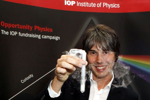
The Institute of Physics (IOP), which publishes Physics World, launched its first-ever fundraising campaign at a dinner at the Institute’s headquarters in London last night. The aim of the campaign, called Opportunity Physics, is to raise £10m over five years to let the Institute “significantly scale up” its work over the coming decades. The evening was hosted by Manchester University particle physicist Brian Cox, who is on the fundraising campaign’s board and is a familiar face as presenter of TV shows such as the BBC’s Wonders of the Solar System.

The Institute says it has identified a number of existing IOP projects that can be enhanced if further funding were available. Those projects are all centred on inspiring young people into physics, showing them what careers physics can lead to, helping physicists to flourish – whether they work in teaching, research or industry – and underlining how physics is central to a healthy, technology-led economy. With 52,000 members, the Institute already does a lot of good work, but it believes it can do even more with additional cash.

(more…)

Scanning tunnelling microscopy and infrared spectroscopy join forces

Physicists in California have combined infrared spectroscopy with scanning tunnelling microscopy to create a new technique that measures the subtle changes that can happen to molecules when they stick to a surface. The method promises to improve our understanding of how molecules behave on surfaces and could be used to help develop better surface catalysts for industrial processes. The team also believes that the technique could be further developed to map the locations of surface molecules on a nanometre scale.

Since its invention in 1981, the scanning tunnelling microscope (STM) has become an important research tool for physicists, chemists and materials scientists. It works by scanning an atomically sharp tip very near to the surface of interest and monitoring the electrical current flowing between the two. While a STM can spot individual atoms and molecules on a surface, it cannot directly distinguish between different chemical species – with two or more very different molecules appearing the same in an STM image.

Infrared spectroscopy, on the other hand, is very good at identifying molecules. It works by shining broadband infrared light onto a sample and each type of molecule that is present is identified by how it absorbs the light at a distinct set of frequencies. But because the technique relies on light with relatively long wavelengths – about 1 μm or longer – it cannot pinpoint the locations of molecules on the nanoscale.

Expand and crash

Several attempts have already been made to combine infrared spectroscopy with a STM. However, they have all had limited success because the infrared light heats the tip, causing it to expand and crash into the surface.

In this latest work, students in Michael Crommie‘s research group at the University of California, Berkeley (UCB) have taken a different approach to this problem. The team used a custom-built tunable infrared laser designed by Feng Wang, who is also at UCB, to irradiate a gold surface that is partially covered with single molecules of either [121]tetramantane or [123]tetramantane. It then positioned the tip of a STM above the gold surface about a millimetre away from the region that was illuminated by the laser. This is far enough away to avoid heating the tip.

The researchers found that when the laser’s frequency equalled one of the absorption frequencies of the adsorbed hydrocarbon, the tunnelling current between surface and tip increased. The team believes this is because when surface molecules absorb infrared light, the energy rapidly dissipates into the gold substrate as heat. This heat, the researchers suggest, causes the gold to expand slightly, thus bringing the surface closer to the needle and increasing the tunnelling current.

Very good resolution

By measuring the precise frequencies at which the tunnelling current increased, the researchers could identify the spectral fingerprints of either [121]tetramantane or [123]tetramantane, allowing them to identify which of the two molecules was adsorbed onto the gold substrate. Furthermore, they found that the spectral resolution of the technique is much better than previous STM-based methods.

By comparing the absorption spectra of molecules on the surface with those of the same molecules in a bulk sample, the team could deduce important information about how the surface-bound molecules interacted with each other and with the substrate.

There is a catch, however. Because the microscope tip has to be placed outside the laser spot, it detects an averaged signal from all the irradiated molecules. “We have not yet been able to perform infrared spectroscopy on a single molecule,” says team-leader Crommie, “but that’s something we want to do in the future.”

I’m really amazed that you can detect the energy from 1 mm away – that’s a distance of millions of atoms
Ludwig Bartels, University of California, Riverside

“I’m really amazed that you can detect the energy from 1 mm away – that’s a distance of millions of atoms,” says Ludwig Bartels, a STM expert at the University of California, Riverside who was not involved in the current research. He believes that the research marks “a paradigm shift in our understanding rather than an incremental increase”. However, he is sceptical of the researchers’ simple explanation that the signal is caused by the expansion of the substrate, saying he would be “truly amazed” if the amount of heat that was transferred to the material by the infrared photons caused detectable expansion 1 mm away. Instead, he suspects a more complex, as-yet-undocumented process might explain the energy transmission through the surface.

He also doubts the researchers’ prospects of achieving single-molecule vibrational spectroscopy using this method, suggesting that the signal from a single molecule would almost certainly be too weak to be detected without bringing the tip so close that it would be heated by the laser. He believes, however, that a proper understanding of how the energy radiates through the surface of the material could potentially have a major impact on the future of microelectronics.

The research is described in Physical Review Letters.

Copyright © 2026 by IOP Publishing Ltd and individual contributors