I’m pleased to welcome you to Physics World’s coverage supporting the International Year of Quantum Science and Technology (IYQ) in 2025. The IYQ is a worldwide celebration, endorsed by the United Nations (UN), to increase the public’s awareness of quantum science and its applications. The year 2025 was chosen as it marks the centenary of the initial development of quantum mechanics by Werner Heisenberg.
With six “founding partners”, including the Institute of Physics (IOP), which publishes Physics World, the IYQ has ambitious aims. It wants to show how quantum science can do everything from grow the economy, support industry and improve our health to help the climate, deliver clean energy and reduce inequalities in education and research. You can join in by creating an event or donating money to the IYQ Global Fund.
Quantum science is burgeoning, with huge advances in basic research and applications such as quantum computing, communication, cryptography and sensors. Countless tech firms are getting in on the act, including giants like Google, IBM and Microsoft as well as start-ups such as Oxford Quantum Circuits, PsiQuantum, Quantinuum, QuEra and Riverlane. Businesses in related areas – from banking to aerospace – are eyeing up the possibilities of quantum tech too.
Where it all began It was on the island of Helgoland off the coast of Germany in June 1925 that Werner Heisenberg created matrix mechanics, commemorated by the International Year of Quantum Science and Technology. (Courtesy: iStock/Iurii Buriak)
An official IYQ opening ceremony will be taking place at UNESCO headquarters in Paris on 4–5 February 2025. Perhaps the highlight of the year for physicists is a workshop from 9–14 June in Helgoland – the tiny island off the coast of Germany where Heisenberg made his breakthrough exactly 100 years ago. Many of the leading lights from quantum physics will be there, including five Nobel-prize winners.
Kicking off our coverage of IYQ, historian Robert P Crease from Stony Brook University has talked to some of the delegates at Helgoland to find out what they hope to achieve at the event. Crease also examines whether Heisenberg’s revelations were as clear-cut as he later claimed. Did he really devise the principles of quantum mechanics at precisely 3 a.m. one June morning 100 years ago?
From a different perspective, Oksana Kondratyeva explains how she has worked with US firm Rigetti Computing to create a piece of stained glass art inspired by the company’s quantum computers – a “quantum rose for the 21st century” as she puts it. You can find out more about her quantum-themed artwork in a special video she’s made.
Stimulated by science Oksana Kondratyeva has created a unique piece of stained-glass art inspired by a Rigetti quantum computer. She is shown here working in a specially equipped studio using highly corrosive hydrofluoric acid to etch the glass. (Courtesy: Oksana Kondratyeva)
Other quantum coverage in 2025 will include special episodes of the Physics World podcasts and Physics World Live. The next edition of Physics World Careers, due out in the new year, has a quantum theme, and there’ll also be a bumper, quantum-themed issue of the Physics World Briefing in May. The Physics World quantum channel will be regularly updated throughout the year so you don’t miss a thing.
Beyond the lab UK firm Oxford Ionics, which is developing quantum computers based on trapped ion qubits, is one of numerous businesses bringing quantum science into real-world applications. (Courtesy: Oxford Ionics)
IOP Publishing, meanwhile, will be bringing out a series of Perspectives articles – personal viewpoints from leading quantum scientists – in Quantum Science and Technology. The journal will also be publishing roadmaps in quantum computing, sensing, communication and simulation, as well as focus issues on topics such as quantum machine learning and technologies for quantum gravity.
There’ll be many other events and initiatives by other organizations too, including from the other founding partners, the American Physical Society, the German Physical Society, Optica, SPIE and the Chinese Optical Society. What’s more, the IYQ is a truly global initiative, with almost 60 nations, led by Ghana and Mexico, helping to get the year off the ground, spreading the benefits of quantum science across the planet, including to the Global South.
The beauty of quantum science lies not only in its mystery but also in the ground-breaking, practical applications that it is inspiring. The IYQ deserves to be a huge success – in fact, I am sure it will.
A new observation of electron and positron cosmic rays has confirmed the existence of what could be a “cooling break” in the energy spectrum at around 1 TeV, beyond which the particle flux decreases more rapidly. Aside from this break, however, the spectrum is featureless, showing no evidence of an apparent anomaly previously associated with a dark matter signal.
Cosmic ray is a generic term for an energetic charged particle that enters Earth’s atmosphere from space. Most cosmic rays are protons, some are heavier nuclei, and a small number (orders of magnitude fewer than protons) are electrons and their antiparticles (positrons).
“Because the electron’s mass is small, they radiate much more effectively than protons,” explains high-energy astrophysicist Felix Aharonian of the Max Planck Institute for Nuclear Physics in Heidelberg, Germany. “It makes the electrons very fragile, so the electrons we detect cannot be very old. That means the sources that produce them cannot be very far away.” Cosmic-ray electrons and positrons can therefore provide important information about our local cosmic environment.
Today, however, the origins of these electrons and positrons are hotly debated. They could be produced by nearby pulsars or supernova remnants. Some astrophysicists favour a secondary production model in which other cosmic rays interact locally with interstellar gas to create high-energy electrons and positrons.
Unexplained features
Previous measurements of the energy spectra of these cosmic rays revealed several unexplained features. In general, the particle flux decreases with increasing energy. At energies below about 1 TeV, the decline is a steady exponential. But at about 1 TeV, the decline steepens with a larger exponential at a curious kink or break point.
Later observations by the Dark Matter Particle Explorer (DAMPE) collaboration confirmed this kink, but also appeared to show peaks at higher energies. Some theoreticians have suggested these inhomogeneities could arise from local sources such as pulsars, whereas others have advanced more exotic explanations, such as signals from dark matter.
In the new work, members of the High Energy Stereoscopic System (HESS) collaboration looked for evidence of cosmic electrons and positrons in 12 years of data from the HESS observatory in Namibia. HESS’s primary mission is to observe high-energy cosmic gamma rays. These gamma rays interact with the atmosphere creating showers of energetic charged particles. These showers create Cherenkov light, which is detected by HESS.
Similar but not identical
The observatory can also detect atmospheric showers created by cosmic rays such as protons and electrons. However, discerning between showers created by protons and electrons/positrons is a significant challenge (HESS cannot differentiate between electrons and positrons). “The hadronic showers produced by protons and electronic showers are extremely similar but not identical,” says Aharonian; “Now we want to use this tiny difference to distinguish between electron-produced showers and proton-produced showers. The task is very difficult because we need to reject proton showers by four orders of magnitude and still keep a reasonable fraction of electrons.”
Fortunately, the large data sample from HESS meant that the team could identify weak signals associated with electrons and positrons. The researchers were therefore able to extend the flux measurements out to much higher energies. Whereas previous surveys could not look higher than about 5 TeV, the HESS researchers probed the 0.3–40 TeV range – although Aharonian concedes that the error bars are “huge” at higher energies.
The study confirms that, up until about 1 TeV, the spectrum decreases exponentially. The team measured this exponent to be about 3.25. At about 1 TeV, a sharp downward kink was also observed – with an exponential decrease of about 4.5 at higher energies. However, there is no sign of any bumps or peaks in the data.
This kink can be naturally explained, says Aharonian, as a “cooling break”, in which the low energy electrons are produced by background processes, whereas the high-energy electrons are produced locally. “Teraelectronvolt electrons can only come from local sources,” he says. In theoretical models, the intensity of both fluxes would decay exponentially, and the difference between the exponents would be 1 – close to that measured here. Aharonian believes that further information about this phenomenon could come from techniques such as machine learning or muon detection to distinguish between high-energy proton showers and electron showers.
“This is a unique measurement: it gives you a value of the electron–positron flux up to extremely high energies,” says Andrei Kounine of Massachusetts Institute of Technology, who works on the Alpha Magnetic Spectrometer (AMS-02) detector on the International Space Station. While he expresses some concerns about possible uncharacterized systematic errors at very high energies, he says they do not meaningfully diminish the value of the HESS team’s work. He notes that there are a variety of unexplained anomalies in the energy spectra of various cosmic-ray particles. “What we are missing at the moment,” he says, “is a comprehensive theory that considers all possible effects and tries to predict from fundamental measurements such as the proton spectrum the fluxes of all other elements.”
Electronic chips are made using photolithography, which involves shining ultraviolet light through a patterned mask and onto a semiconductor wafer. The light activates a photoresist on the surface, which allows the etching of a pattern on the wafer. Through successive iterations of photolithography and the deposition of metals, devices with features as small as a few dozen nanometres are created.
Crucial to this complex manufacturing process is aligning the wafer with successive masks. This must be done in a rapid and repeatable manner, while maintaining nanometre precision throughout the manufacturing process. That’s where Queensgate – part of precision optical and mechanical instrumentation manufacturer Prior Scientific – comes into the picture.
For 45 years, UK-based Queensgate has led the way in the development of nanopositioning technologies. The firm spun out of Imperial College London in 1979 as a supplier of precision instrumentation for astronomy. Its global reputation was sealed when NASA chose Queensgate technology for use on the Space Shuttle and the International Space Station. The company has worked for over two decades with the hard-disk drive-maker Seagate to develop technologies for the rapid inspection of read/write heads during manufacture. Queensgate is also involved in a longstanding collaboration with the UK’s National Physical Laboratory (NPL) to develop nanopositioning technologies that are being used to define international standards of measurement.
Move to larger wafers
The semiconductor industry is in the process of moving from 200 mm to 300 mm wafers – which doubles the number of chips that can be produced from a wafer. Processing the larger and heavier wafers requires a new generation of equipment that can position wafers at nanometre precision.
Queensgate already works with original equipment manufacturers (OEMs) to make optical wafer-inspection systems that are used to identify defects during the processing of 300 mm wafers. Now the company has set its sights on wafer alignment systems. The move to 300 mm wafers offers the company an opportunity to contribute to the development the next-generation alignment systems – says Queensgate product manager Craig Goodman.
Craig Goodman (Courtesy: Queensgate)
“The wafers are getting bigger, which puts a bigger strain on the positioning requirements and we’re here to help solve problems that that’s causing,” explains Goodman. “We are getting lots of inquiries from OEMs about how our technology can be used in the precision positioning of wafers used to produce next-generation high-performance semiconductor devices”.
The move to 300 mm means that fabs need to align wafers that are both larger in area and much heavier. What is more, a much heavier chuck is required to hold a 300 mm wafer during production. This leads to conflicting requirements for a positioning system. It must be accurate over shorter distances as feature sizes shrink, but also be capable of moving a much larger and much heavier wafer and chuck. Today, Queensgate’s wafer stage can handle wafers weighing up to 14 kg while achieving a spatial resolution of 1.5 nm.
Goodman explains that Queensgate’s technology is not used to make large adjustments in the relative alignment of wafer and mask – which is done by longer travel stages using technologies such as air-bearings. Instead, the firm’s nanopositioning systems are used in the final stage of alignment, moving the wafer by less than 1 mm at nanometre precision.
Eliminating noise
Achieving this precision was a huge challenge that Queensgate has overcome by focusing on the sources of noise in its nanopositioning systems. Goodman says that there are two main types of noise that must be minimized. One is external vibration, which can come from a range of environmental sources – even human voices. The other is noise in the electronics that control the nanopositioning system’s piezoelectric actuators.
Goodman explains that noise reduction is achieved through the clever design of the mechanical and electronic systems used for nanopositioning. The positioning stage, for example, must be stiff to reject vibrational noise and notch filters are used to minimize the effect of electronic noise to the sub-nanometre level.
Queensgate provides its nanopostioning technology to OEMs, who integrate it within their products – which are then sold to chipmakers. Goodman says that Queensgate works in-house with its OEM customers to ensure that the desired specifications are achieved. “A stage or a positioner for 300 mm wafers is a highly customized application of our technologies,” he explains.
While the resulting nanopositioning systems are state of the art, Goodman points out that they will be used in huge facilities that process tens of thousands of wafers per month. “It is our aim and our customer’s aim that Queensgate nanopositioning technologies will be used in the mass manufacture of chips,” says Goodman. This means that the system must be very fast to achieve high throughput. “That is why we are using piezoelectric actuators for the final micron of positioning – they are very fast and very precise.”
Today most chip manufacturing is done in Asia, but there are ongoing efforts to boost production in the US and Europe to ensure secure supplies in the future. Goodman says this trend to semiconductor independence is an important opportunity for Queensgate. “It’s a highly competitive, growing and interesting market to be a part of,” he says.
The datasheet for Queensgate’s NPS-XYP-250Q 300 mm wafer–mask alignment stage is now available. Goodman describes it as, “the physically ‘largest’ piezo nanopositioning stage ever delivered”.
On Christmas Day in 1741, when Swedish scientist Anders Celsius first noted down the temperature in his Uppsala observatory using his own 100-point – or “Centi-grade” – scale, he would have had no idea that this was to be his greatest legacy.
A newly published, engrossing biography – Celsius:a Life and Death by Degrees – by Ian Hembrow, tells the life story of the man whose name is so well known. The book reveals the broader scope of Celsius’ scientific contributions beyond the famous centigrade scale, as well as highlighting the collaborative nature of scientific endeavours, and drawing parallels to modern scientific challenges such as climate change.
That winter, Celsius, who was at the time in his early 40s, was making repeated measurements of the period of a pendulum – the time it takes for one complete swing back and forth. He could use that to calculate a precise value for the acceleration caused by gravity, and he was expecting to find that value to be very slightly greater in Sweden than at more southern latitudes. That would provide further evidence for the flattening of the Earth at the poles, something that Celsius had already helped establish. But it required great precision in the experimental work, and Celsius was worried that the length (and therefore the period) of the pendulum would vary slightly with temperature. He had started these measurements that summer and now it was winter, which meant he had lit a fire to hopefully match the summer temperatures. But would that suffice?
Throughout his career, Celsius had been a champion of precise measurement, and he knew that temperature readings were often far from precise. He was using a thermometer sent to him by the French astronomer Joseph-Nicolas Delisle, with a design based on the expansion of mercury. That method was promising, but Delisle used a scale that took the boiling point of water and the temperature in the basement of his home in Paris as its tworeference points. Celsius was unconvinced by the latter. So he made adaptations (which are still there to be seen in an Uppsala museum), twisting wire around the glass tube at the boiling and freezing points of water, and dividing the length between the two into 100 even steps.
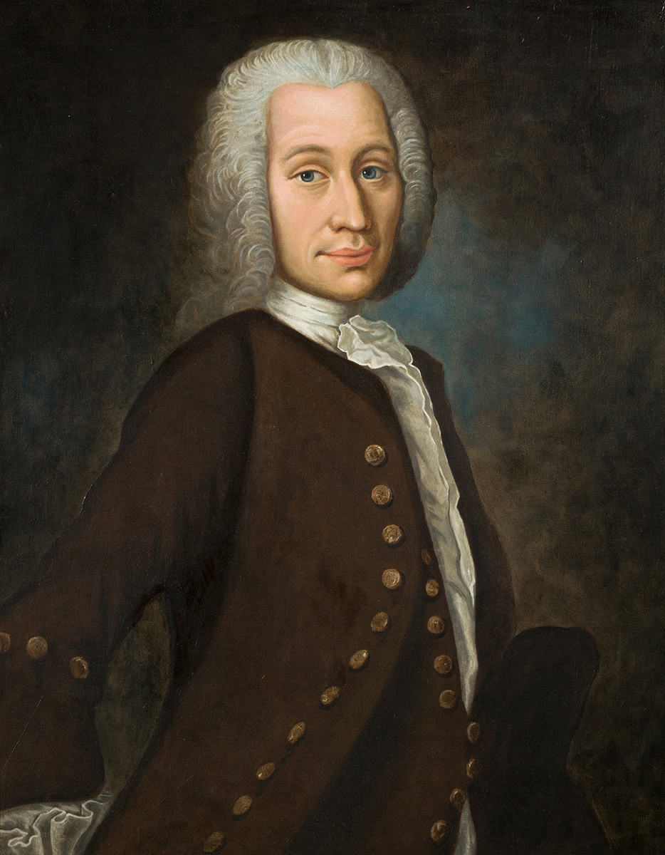
Man of scale Anders Celsius, painted by Magnus Bratt. Copy of Olof Arenius’s portrait of Celsius, which is at the Astronomical Observatory in Uppsala, Sweden. (Courtesy: Museum Gustavianum, photograph by Mikael Wallerstedt)
The centigrade scale, later renamed in his honour, was born. In his first recorded readings he found the temperature in the pleasantly heated room to be a little over 80 degrees! Following Delisle’s system – perhaps noting that this would mean he had to do less work with negative numbers – he placed the boiling point at zero on his scale, and the freezing point at 100. It was some years later, after his death, that a scientific consensus flipped the scale on its head to create the version we know so well today.
Hembrow does a great job at placing this moment in the context of the time, and within the context of Celsius’ life. He spends considerable time recounting the scientist’s many other achievements and the milestones of his fascinating life.
The expedition that had established the flattening of the Earth at the poles was the culmination of a four-year grand tour that Celsius had undertaken in his early 30s. Already a professor at Uppsala University, in the town where he had grown up in an academic family, he travelled to Germany, Italy, France and London. There he saw at first hand the great observatories that he had heard of and established links with the people who had built and maintained them.
On his extended travels he became a respected figure in the world of science and so it was no surprise when he was selected to join a French expedition to the Arctic in 1736, led by mathematician Pierre Louis Maupertuis, to measure a degree of latitude. Isaac Newton had died just a few years before and his ideas relating to gravitation were not yet universally accepted. If it could be shown that the distance between two lines of latitude was greater near the poles than on the equator, that would prove Newton right about the shape of the Earth, a key prediction of his theory of gravitation.
After a period of time in London equipping themselves with the precision instruments, the team started the arduous journey to the Far North. Once there they had to survey the land – a task made challenging by the thick forest and hilly territory. They selected nine mountains to climb with their heavy equipment, felling dozens of trees on each and then creating a sturdy wooden marker on each peak. This allowed them to create a network of triangles stretching north, with each point visible from the two next to it. But they also needed one straight line of known length to complete their calculations. With his local knowledge, Celsius knew that this could only be achieved on the frozen surface of the Torne river – and that it would involve several weeks of living on the ice, working largely in the dark and the intense cold, and sleeping in tents.
After months of hardship, the calculations were complete and showed that the length of one degree of latitude in the Arctic was almost 1.5 km longer than the equivalent value in France. The spheroid shape of the Earth had been established.
Of course, not everybody accepted the result. Politics and personalities got in the way. Hembrow uses this as the starting point for a polemic about aspects of modern science and climate change with which he ends his fine book. He argues that the painstaking work carried out by an international team, willing to share ideas and learn from each other, provides us with a template by which modern problems must be addressed.
Considering how often we use his name, most of us know little about Celsius. This book helps to address that deficit. It is a very enjoyable and accessible read and would appeal, I think, to anybody with an interest in the history of science.
A new transistor made from semiconducting vertical nanowires of gallium antimonide (GaSb) and indium arsenide (InAs) could rival today’s best silicon-based devices. The new transistors are switched on and off by electrons tunnelling through an energy barrier, making them highly energy-efficient. According to their developers at the Massachusetts Institute of Technology (MIT) in the US, they could be ideal for low-energy applications such as the Internet of Things (IoT).
Electronic transistors use an applied voltage to regulate the flow of electricity – that is, electrons – within a semiconductor chip. When this voltage is applied to a conventional silicon transistor, electrons climb over an energy barrier from one side of the device to the other, and it switches from an “off” state to an “on” one. This type of switching is the basis of modern information technology, but there is a fundamental physical limit on the threshold voltage required to get the electrons moving. This limit, which is sometimes termed the “Boltzmann tyranny” because it stems from the Boltzmann-like energy distribution of electrons in a semiconductor, puts a cap on the energy efficiency of this type of transistor.
Highly precise process
In the new work, MIT researchers led by electrical engineer Jesús A del Alamo made their transistor using a top-down fabrication technique they developed. This extremely precise process uses high-quality, epitaxially-grown structures and both dry and wet etching to fabricate nanowires just 6 nm in diameter. The researchers then placed a gate stack composed of a very thin gate dielectric and a metal gate on the sidewalls of the nanowires. Finally, they added point contacts to the source, gate and drain of the transistors using multiple planarization and etch-back steps.
The sub-10 nm size of the devices and the extreme thinness of the gate dielectric (just 2.4 nm) means that electrons are confined in a space so small that they can no longer move freely. In this quantum confinement regime, electrons no longer climb over the thin energy barrier at the GaSb/InAs heterojunction. Instead, they tunnel through it. The voltage required for such a device to switch is much lower than it is for traditional silicon-based transistors.
Steep switching slope and high drive current
Researchers have been studying tunnelling-type transistors for more than 20 years, notes Yanjie Shao, a postdoctoral researcher in nanoelectronics and semiconductor physics at MIT and the lead author of a study in Nature Electronics on the new transistor. Such devices are considered attractive because they allow for ultra-low-power electronics. However, they come with a major challenge: it is hard to maintain a sharp transition between “off” and “on” while delivering a high drive current.
When the project began five years ago, Shao says the team “believed in the potential of the GaSb/InAs ‘broken-band’ system to overcome this difficulty”. But it wasn’t all plain sailing. Fabricating such small vertical nanowires was, he says, “one of the biggest problems we faced”. Making a high-quality gate stack with a very low density of electronic trap states (states within dielectric materials that capture and release charge carriers in a semiconductor channel) was another challenge.
After many unsuccessful attempts, the team found a way to make the system work. “We devised a plasma-enhanced deposition method to make the gate electric and this was key to obtaining exciting transistor performance,” Shao tells Physics World.
The researchers also needed to understand the behaviour of tunnelling transistors, which Shao calls “not easy”. The task was made possible, he adds, by a combination of experimental work and first-principles modelling by Ju Li’s group at MIT, together with quantum transport simulation by David Esseni’s group at the University of Udine, Italy. These studies revealed that band alignment and near-periphery scaling of the number of conduction modes at the heterojunction interface play key roles in the physics of electrons under extreme confinement.
The reward for all this work is a device with a drive current as high as 300 uA/m and a switching slope less than 60 mV/decade (a decade, in this context, is a power of 10 difference between off and on states), meaning that the supply voltage is just 0.3 V. This is below the fundamental limit achievable with silicon-based devices, and around 20 times better than other tunnelling transistors of its type.
Potential for novel devices
Shao says the most likely applications for the new transistor are in ultra-low-voltage electronics. These will be useful for artificial intelligence and Internet of Things (IoT) applications, which require devices with higher energy efficiencies. Shao also hopes the team’s work will bring about a better understanding of the physics at surfaces and interfaces that feature extreme quantum confinement – something that could lead to novel devices that benefit from such nanoscale physics.
The MIT team is now developing transistors with a slightly different configuration that features vertical “nano-fins”. These could make it possible to build more uniform devices with less structural variation across the surface. “Being so small, even a variation of just 1 nm can adversely affect their operation,” Shao says. “We also hope that we can bring this technology closer to real manufacturing by optimizing the process technology.”
Physical exercise plays an important role in controlling disease, including cancer, due to its effect on the human body’s immune system. A research team from the USA and India has now developed a mathematical model to quantitatively investigate the complex relationship between exercise, immune function and cancer.
Exercise is thought to supress tumour growth by activating the body’s natural killer (NK) cells. In particular, skeletal muscle contractions drive the release of interleukin-6 (IL-6), which causes NK cells to shift from an inactive to an active state. The activated NK cells can then infiltrate and kill tumour cells. To investigate this process in more depth, the team developed a mathematical model describing the transition of a NK cell from its inactive to active state, at a rate driven by exercise-induced IL-6 levels.
“We developed this model to study how the interplay of exercise intensity and exercise duration can lead to tumour suppression and how the parameters associated with these exercise features can be tuned to get optimal suppression,” explains senior author Niraj Kumar from the University of Massachusetts Boston.
Impact of exercise intensity and duration
The model, reported in Physical Biology, is constructed from three ordinary differential equations that describe the temporal evolution of the number of inactive NK cells, active NK cells and tumour cells, as functions of the growth rates, death rates, switching rates (for NK cells) and the rate of tumour cell kill by activated NK cells.
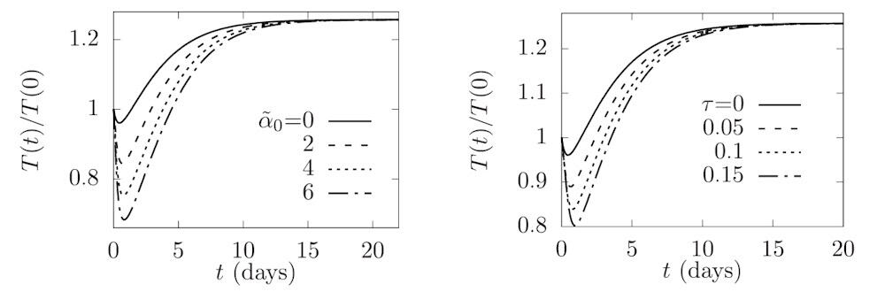
Kumar and collaborators – Jay Taylor at Northeastern University and T Bagarti at Tata Steel’s Graphene Center – first investigated how exercise intensity impacts tumour suppression. They used their model to determine the evolution over time of tumour cells for different values of α0 – a parameter that correlates with the maximum level of IL-6 and increases with increased exercise intensity.
Modelling suppression Temporal evolution of tumour cells for different values of α0 (left) and exercise time scale τ (right). (Courtesy: J Taylor et al Phys. Biol. 10.1088/1478-3975/ad899d)
Simulating tumour growth over 20 days showed that the tumour population increased non-monotonically, exhibiting a minimum population (maximum tumour suppression) at a certain critical time before increasing and then reaching a steady-state value in the long term. At all time points, the largest tumour population was seen for the no-exercise case, confirming the premise that exercise helps suppress tumour growth.
The model revealed that as the intensity of the exercise increased, the level of tumour suppression increased alongside, due to the larger number of active NK cells. In addition, greater exercise intensity sustained tumour suppression for a longer time. The researchers also observed that if the initial tumour population was closer to the steady state, the effect of exercise on tumour suppression was reduced.
Next, the team examined the effect of exercise duration, by calculating tumour evolution over time for varying exercise time scales. Again, the tumour population showed non-monotonic growth with a minimum population at a certain critical time and a maximum population in the no-exercise case. The maximum level of tumour suppression increased with increasing exercise duration.
Finally, the researchers analysed how multiple bouts of exercise impact tumour suppression, modelling a series of alternating exercise and rest periods. The model revealed that the effect of exercise on maximum tumour suppression exhibits a threshold response with exercise frequency. Up to a critical frequency, which varies with exercise intensity, the maximum tumour suppression doesn’t change. However, if the exercise frequency exceeds the critical frequency, it leads to a corresponding increase in maximum tumour suppression.
Clinical potential
Overall, the model demonstrated that increasing the intensity or duration of exercise leads to greater and sustained tumour suppression. It also showed that manipulating exercise frequency and intensity within multiple exercise bouts had a pronounced effect on tumour evolution.
These results highlight the model’s potential to guide the integration of exercise into a patient’s cancer treatment programme. While still at the early development stage, the model offers valuable insight into how exercise can influence immune responses. And as Taylor points out, as more experimental data become available, the model has potential for further extension.
“In the future, the model could be adapted for clinical use by testing its predictions in human trials,” he explains. “For now, it provides a foundation for designing exercise regimens that could optimize immune function and tumour suppression in cancer patients, based on the exercise intensity and duration.”
Next, the researchers plan to extend the model to incorporate both exercise and chemotherapy dosing. They will also explore how heterogeneity in the tumour population can influence tumour suppression.
The US Department of Energy (DOE) has awarded $50m to a consortium of national laboratories and universities to develop sodium-ion batteries as a sustainable, low-cost alternative to lithium-ion technology.
Lithium-ion batteries currently dominate the electric-vehicle market and they are also used in smartphones and to store energy from renewable source such as wind and solar. Yet relying on a single battery technology such as lithium-ion creates dependencies on critical elements such as lithium, cobalt and nickel.
Sodium, however, is an abundant, inexpensive element and offers a promising way to diversify battery materials. The downside is that sodium-ion batteries currently store less energy per unit weight and volume than lithium-ion batteries.
The money from the DOE over the next five years will be used to create the Low-cost Earth-abundant Na-ion Storage (LENS) consortium. LENS will be led by Argonne National Laboratory and includes five other DOE national laboratories such as Brookhaven, Lawrence Berkely and Sandia as well eight US universities.
“By leading the LENS consortium, Argonne will push sodium-ion battery technology forward and contribute to a secure energy future for everyone,” notes Argonne director Paul Kearns. “Our scientific expertise and dynamic collaborations in this important field will strengthen US competitiveness.”
The LENS consortium will now develop high-energy electrode materials and electrolytes for sodium-ion batteries as well as design, integrate and benchmark battery cells with the aim of creating high-energy, long-lasting batteries.
“The challenge ahead is improving sodium-ion energy density so that it first matches and then exceeds that of phosphate-based lithium-ion batteries while minimizing and eliminating the use of all critical elements,” says LENS consortium director Venkat Srinivasan.
Venkat Srinivasan, William Mustain and Martin Freer appeared on a Physics World Live panel discussion about battery technology held on 21 November 2024, which you can watch online now
Stained glass is the most “physical” of all art forms. If you’ve ever been inside Chartres Cathedral in France or York Minster in the UK, you’ll know how such glass can transform a building by turning sunlight into gloriously captivating multicoloured patterns. What you might not realize, however, is that centuries of scientific innovation have forged this form of art.
Byzantine glaziers started making leaded glass windows back in the 6th century CE before the technique spread widely across Europe. But our ability to stain glass only emerged in the 14th century when medieval alchemists found that coating glass with silver nitrate and firing it in a kiln gave the material a range of orange and yellow hues.
Later, a range of other techniques were developed to produce various decorative effects, with stained glass becoming both an art and a craft. Particularly important has been the use of hydrofluoric acid – a poisonous and highly corrosive liquid – to strip off the surface of glass, layer by layer, to alter its colour and thickness.
Known as hydrofluoric acid etching, the technique is widely used by modern architectural glass artists. Beautiful patterns can be created by altering the strength and temperature of the acid and varying the time for which the glass is exposed to it. Materials like wax, bitumen and lead foil can also be used as resists to leave parts of the glass untouched.
Like other “glass artists”, I am an experimentalist of sorts. We use an empirical knowledge of glass to make beautiful objects – and sometimes even make new discoveries
Like other “glass artists”, I am an experimentalist of sorts. We use an empirical knowledge of glass to make beautiful objects – and sometimes even make new discoveries. In fact, some historians say that hydrofluoric acid was first created in 1670 by a German glassworker named Heinrich Schwanhardt.
While treating a mineral called fluorspar with acid, he saw that the lenses in his spectacles went cloudy – prompting him to start using the same reaction to etch glass. Only much later – in the late 18th century – did chemists carry out “proper” lab experiments to show that fluorspar (calcium fluoride) reacts with the acid to create what we now call hydrofluoric acid.
From the 19th century onwards, acid-etching techniques started to be used by numerous stained-glass artists and studios throughout Britain and Ireland. Dublin-born Harry Clarke (1889–1931) was the leading proponent of the hydrofluoric acid-etching technique, which he mastered in an exceptionally personal and imaginative manner.
Art of glass
I first came across acid etching in 2010 while studying glass and architecture at Central Saint Martins, which is part of the University of the Arts London. The technique intrigued me and I started wondering about its origins and how it works, from a scientific point of view. What chemical processes are involved? What happens if you vary how the acid is applied? And how can that create new decorative effects?
Meet the artPer scientiam ad astra by Oksana Kondratyeva on display at the Ruskin Glass Centre in the UK, home to the 2024 British Glass Biennale in Stourbridge, near Birmingham, UK. (Courtesy: Oksana Kondratyeva)
Unable to find full answers to my questions, I started carrying out my own experiments and investigations. I wanted to understand how fluorspar – which can be colourless, deep green or even purple – can be turned into hydrofluoric acid and what goes on at a chemical level when it etches glass.
During my investigations, which I published in 2014 in The Journal of Stained Glass (38 146), I was astonished to find references to glass in the famous lectures given by Richard Feynman about quantum electrodynamics. Published in book form as QED: the Strange Theory of Light and Matter, Feynman explained the partial reflection of light by experimenting with blocks of glass.
He showed that the amount of light reflected increases with the thickness of the glass, pointing out that photons interact with electrons throughout the material, not just on the surface. “A piece of glass,” Feynman wrote, “is a terrible monster of complexity – huge numbers of electrons are jiggling about.”
In my own work, I’ve recently been experimenting with glass of different thickness to make a piece of art inspired by the packaging for a quantum chip made by Rigetti Computing. Entitled Per scientiam ad astra (through science to the stars), the artwork was displayed at the 2024 British Glass Biennale at the Ruskin Glass Centre in Stourbridge, UK – a historically significant area for glass-making that pioneered the creation of etched glass in the 19th century.
Rigetti Computing’s quantum chip
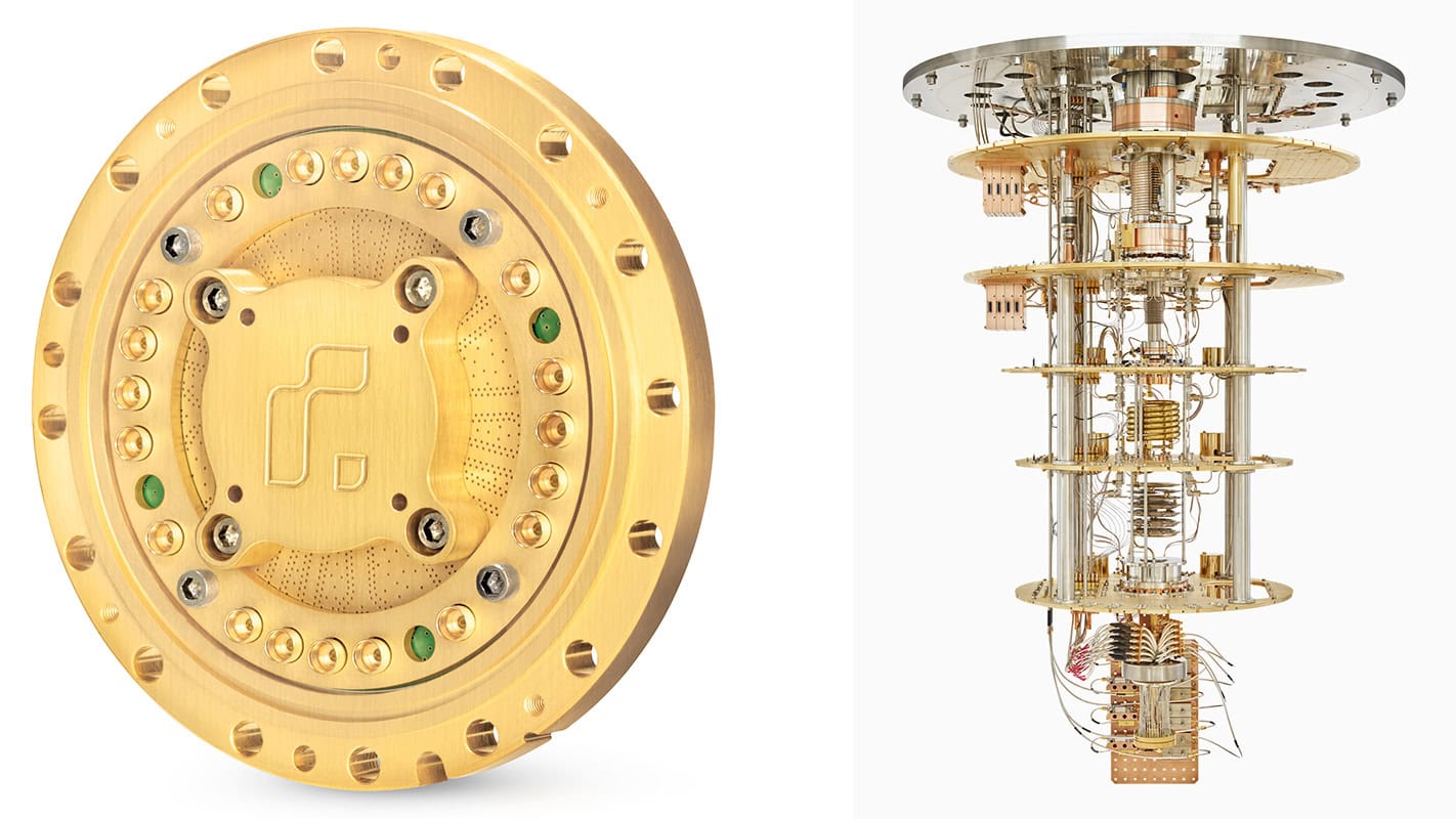
Art from science (left) The packaging for Rigetti Computing’s quantum chip that inspired the stained-glass artwork made by Oksana Kondratyeva. (right) The Rigetti quantum computer, with packaging visible at the bottom attached to the input/output plate. (Courtesy: Rigetti Computing)
The quantum computers developed by US firm Rigetti Computing are based on superconducting qubits made from materials such as aluminium, indium and niobium. The qubits are manufactured using a mix of novel fabrication methods and well-established semiconductor and micro-electromechanical systems (MEMS) processing techniques. The quantum chip – containing the qubits and other components such as readout resonators – are carefully assembled inside a gold-plated copper packaging that connects it to a printed circuit board (PCB).
The PCB in turn routes the signals to microwave connectors, with the whole system cooled to below 10 millikelvin using dilution refrigeration. The environment in which the quantum bits operate is carefully engineered so that they don’t lose their coherence. Rigetti’s design could, in principle, be scaled up to create much larger and more reliable quantum processors with many more qubits.
The packaging for the quantum chip, on which Oksana Kondratyeva’s artwork is based, is a disc 81.5 mm in diameter and 12 mm deep (see image). With the chip at its centre, the packaging is mounted at the bottom of a tower-like structure that, along with the rest of the fridge and wiring, forms the fully assembled quantum computer. Signals are delivered to and from the chip to drive qubit operations and return measured results.
A quantum rose
Creating an artwork based on quantum technology might be an unusual thing to do, but when I saw a photo of the packaging for a quantum chip back in 2020, I was astounded by the elegant geometry of this enigmatic object, which holds the “brain” of the company’s quantum computer (see box above). Reminding me of the beautiful circular rose windows of medieval cathedrals, I wanted to use glass to create a “quantum rose” for the 21st century. Later, Rigetti got in touch with me after my plans were reported on in Physics World in June 2022.
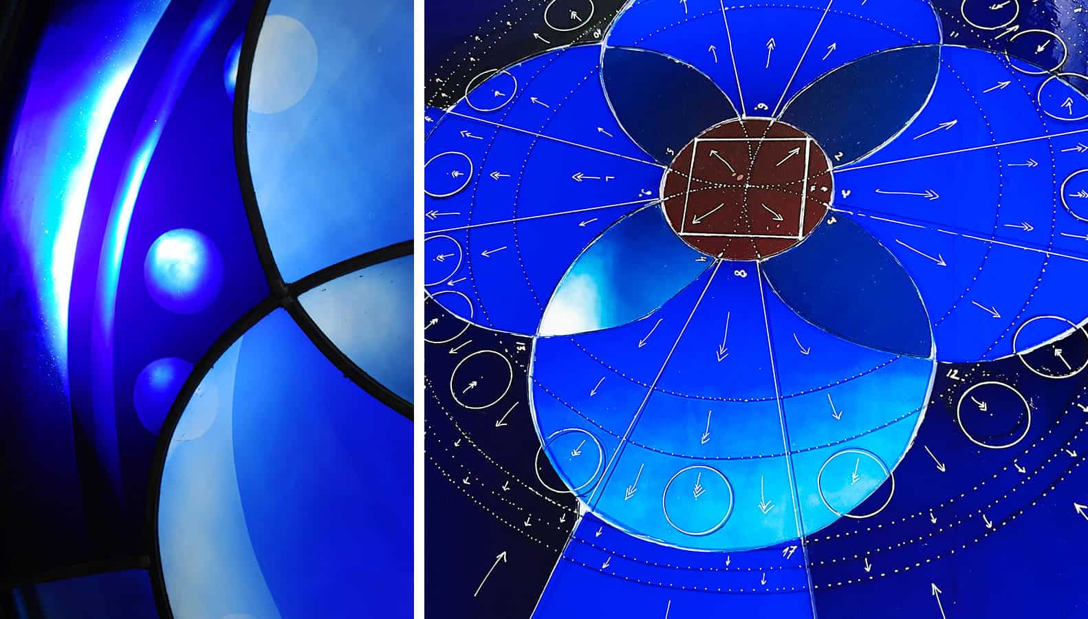
A closer look (left) Per scientiam ad astra was created by Oksana Kondratyeva etching mouth-blown glass with hydrofluoric acid. Each fragment of the artwork was individually acid-etched and leaded. (right) The arrows are “vectors of light” that were temporarily marked by Kondratyeva onto the glass as a guide for the layered acid-etching, reflecting her artistic thought. (Courtesy: Oksana Kondratyeva)
As you can imagine, hydrofluoric acid etching is an extremely dangerous technique, given how corrosive the liquid is. I acid-etch glass from the German company LambertsGlas in a specially equipped studio with a ventilation cabinet to extract fumes and I wear a protective suit with a respiratory mask. As you can see from the video below, I look more like an astronaut than an artist.
Acid etching can be done in lots of different ways (see Materials Today Proceedings55 56) – but I prefer to apply the acid freely with a cotton or plastic brush, coining my technique “acid painting”. The resulting artwork, which took me several months to make, is just over a metre in diameter.
This video has no voice over. (Video courtesy: Space Production)
Mostly blue with a red focal point, the artwork constantly changes as you move around it. Visitors to the British Glass Biennale seemed to be attracted to it, with comments such as “empowering” and “ethereal”. Per scientiam ad astra will now move to a private residence that just happens to be not far from the UK’s National Quantum Computing Centre in Oxfordshire, where one of Rigetti’s quantum computers is housed.
Art–science crossover
Stained-glass windows were once “illuminated books” for people who could not read – mysterious transmitters of knowledge that told stories about human life. The same, in a way, is true of quantum computers, which are broadening our understanding of reality. And just as mathematical equations can have an inner beauty, so too do quantum computers through the myriad technological innovations that underpin them.
With 2025 being the International Year of Quantum Science and Technology, I hope my artwork raises interesting questions at the intersection between art and science, continuing the “two-cultures” dialogue introduced by C P Snow in 1959. Is it a metaphorical window into the secret architecture of the universe? Or is it a visualization of our reality, where Newtonian and quantum-mechanical worlds merge?
Working with stained glass requires an understanding of how materials behave but that knowledge will only get you so far. To reveal new regions of reality and its beauty, unexpectedness plays a role too. Stained-glass art is the convergence of certainty and uncertainty, where science and art come together. Art can unite people; and through the beauty in art, we can create a better reality.
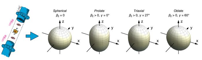
Shape shifter: The nucleus of the xenon atom can assume different shapes depending on the balance of internal forces at play. When two xenon atoms collide at the LHC, simulations indicate that the extremely hot conditions will trigger changes in these shapes. (Courtesy: You Zhou, NBI)
Xenon nuclei change shape as they collide, transforming from soft, oval-shaped particles to rigid, spherical ones. This finding, which is based on simulations of experiments at CERN’s Large Hadron Collider (LHC), provides a first look at how the shapes of atomic nuclei respond to extreme conditions. While the technique is still at the theoretical stage, physicists at the Niels Bohr Institute (NBI) in Denmark and Peking University in China say that ultra-relativistic nuclear collisions at the LHC could allow for the first experimental observations of these so-called nuclear shape phase transitions.
The nucleus of an atom is made up of protons and neutrons, which are collectively known as nucleons. Like electrons, nucleons exist in different energy levels, or shells. To minimize the energy of the system, these shells take different shapes, with possibilities including pear, spherical, oval or peanut-shell-like formations. These shapes affect many properties of the atomic nucleus as well as nuclear processes such as the strong interactions between protons and neutrons. Being able to identify them is thus very useful for predicting how nuclei will behave.
Colliding pairs of 129Xe atoms at the LHC
In the new work, a team led by You Zhou at the NBI and Huichao Song at Peking University studied xenon-129 (129Xe). This isotope has 54 protons and 75 neutrons and is considered a relatively large atom, making its nuclear shape easier, in principle, to study than that of smaller atoms.
Usually, the nucleus of xenon-129 is oval-shaped (technically, it is a 𝛾-soft rotor). However, low-energy nuclear theory predicts that it can transition to a spherical, prolate or oblate shape under certain conditions. “We propose that to probe this change (called a shape phase transition), we could collide pairs of 129Xe atoms at the LHC and use the information we obtain to extract the geometry and shape of the initial colliding nuclei,” Zhou explains. “Probing these initial conditions would then reveal the shape of the 129Xe atoms after they had collided.”
A quark-gluon plasma
To test the viability of such experiments, the researchers simulated accelerating atoms to near relativistic speeds, equivalent to the energies involved in a typical particle-physics experiment at the LHC. At these energies, when nuclei collide with each other, their constituent protons and neutrons break down into smaller particles. These smaller particles are mainly quarks and gluons, and together they form a quark-gluon plasma, which is a liquid with virtually no viscosity.
Zhou, Song and colleagues modelled the properties of this “almost perfect” liquid using an advanced hydrodynamic model they developed called IBBE-VISHNU. According to these analyses, the Xe nuclei go from being soft and oval-shaped to rigid and spherical as they collide.
Studying shape transitions was not initially part of the researchers’ plan. The original aim of their work was to study conditions that prevailed in the first 10-6 seconds after the Big Bang, when the very early universe is thought to have been filled with a quark-gluon plasma of the type produced at the LHC. But after they realized that their simulations could shed light on a different topic, they shifted course.
“Our new study was initiated to address the open question of how nuclear shape transitions manifest in high-energy collisions,” Zhou explains, “and we also wanted to provide experimental insights into existing theoretical nuclear structure predictions.”
One of the team’s greatest difficulties lay in developing the complex models required to account for nuclear deformation and probe the structure of xenon and its fluctuations, Zhou tells Physics World. “There was also a need for compelling new observables that allow for a direct probe of the shape of the colliding nuclei,” he says.
Applications in both high- and low-energy nuclear and structure physics
The work could advance our understanding of fundamental nuclear properties and the operation of the theory of quantum chromodynamics (QCD) under extreme conditions, Zhou adds. “The insights gleaned from this work could guide future nuclear collision experiments and influence our understanding of nuclear phase transitions, with applications extending to both high-energy nuclear physics and low-energy nuclear structure physics,” he says.
The NBI/Peking University researchers say that future experiments could validate the nuclear shape phase transitions they observed in their simulations. Expanding the study to other nuclei that could be collided at the LHC is also on the cards, says Zhou. “This could deepen our understanding of nuclear structure at ultra-short timescales of 10-24 seconds.”
I have mentioned many times in this column the value of the business awards given by the Institute of Physics (IOP), which can be a real “stamp of approval” for firms developing new technology. Having helped to select the 2024 winners, it was great to see eight companies winning a main IOP Business Innovation Award this time round, bringing the total number of firms honoured over the last 13 years to 86. Some have won awards on more than one occasion, with Fetu being one of the latest to join this elite group.
Set up by Jonathan Fenton in 2016, FeTu originally won an IOP Business Start-up Award in 2020 for its innovative Fenton Turbine. According to Fenton, who is chief executive, it is the closest we have ever got to the ideal, closed-cycle reversible heat engine first imagined by thermodynamics pioneer Nicolas Carnot in 1824. The turbine, the firm claims, could replace compressors, air conditioners, fridges, vacuum pumps and heat pumps with efficiency savings across the board.
Back in 2020, it might have sounded like a “too-good-to-be-true” technology, but Fenton has sensibly set out to prove that’s not the case, with some remarkable results. The turbine is complex to describe but the first version promised to cut the energy cost of compressing gases like air by 25%. They claim has already been proven in independent tests carried out by researchers at the University of Bath.
One challenge of any technology with many different applications is picking which to focus on first
One challenge of any technology with many different applications is picking which to focus on first. Having decided to focus on a couple of unique selling factors in large markets, FeTu has now won a 2024 Business Innovation Award for developing a revolutionary heat engine that can generate electrical power from waste heat and geothermal sources as low as 40 °C. It has a huge market potential as it is currently not possible to do this economically.
Innovative ideas
Another winner of an IOP Business Innovation Award is Oxford Ionics, a quantum-computing firm set up in 2019 by Chris Balance and Tom Harty after doing PhDs at the University of Oxford. Their firm’s qubits are based on trapped ions, which traditionally have been controlled with lasers. It’s an approach that works well for small processors, but becomes untenable and error-prone as the size of the processor scales, and the number of qubits increases.
Instead of lasers, Oxford Ionics’ trapped-ion processors use a proprietary, patented electronic system to control the qubits. It was for this system that the company was recognized by the IOP, along with its ability to scale the architecture so that the chips can be made in large quantities on standard semiconductor production lines. That’s essential if we are to build practical quantum computers.
While it’s still early days in the commercialisation of quantum computing, Oxford Ionics is an exciting company to watch. It has already won contracts to supply the UK’s National Quantum Computing Centre at Harwell and has bagged a large contract with its partner Infineon Technologies AG in Munich to build a state-of-the-art portable quantum computer for Germany’s cybersecurity innovation agency. The two firms are one of three independent contractors selected by the agency, which is investing a total of €35m in the project.
I should also mention Dublin-based Equal1, which won the IOP’s £10,000 quantum Business Innovation and Growth (qBIG) Prize in 2024. Equal1 is developing rack-mountable quantum computers powered by a system that integrates quantum and classical components onto a single silicon chip using commercial fabrication processes. The company, which aims to develop compact quantum computers, also won 10 months of mentoring from the award’s sponsors Quantum Exponential.
Meanwhile, Covesion – a photonics and quantum components supplier founded in 2009 – has won an IOP Business Innovation Award for its magnesium-doped, periodically poled, lithium niobate (MgO:PPLN) crystals and waveguides. They allow light to be easily converted from one frequency to another, providing access to wavelengths that are not available from commercial laser sources.
With a manufacturing base in Southampton, Covesion works with customers and industry partners to help them design and make high quality MgO:PPLN products used in a wide range of applications. They include quantum computing, communication, sensing and timing; frequency doubling of femtosecond lasers; mid-infrared generation; atom cooling; terahertz generation and biomedical imaging. The shear breadth and global nature of the customer base is impressive.
Sounds promising
Among the companies to win an IOP Business Start-up Award is Metasonixx, based in Brighton. Spun off from the universities of Bristol and Sussex in 2019, the firm makes mass-produced acoustic metamaterial panels, which can dramatically attenuate sound (10 dB in its Sonoblind) and yet still allow air to flow freely (3 dB or 50% attenuation). That might seem counter-intuitive, but that’s where the innovation comes in and the panels can help with noise management and ventilation, allowing industrial ventilators and heat pumps to be more widely used.
Sounds good Metasonixx is turning metamaterials into commercial reality as noise-abatement products. (Courtesy: Metasonixx Sonoblind Air)
The company really got going in 2020, when it got a grant from UK Research and Innovation to see if its metamaterials could cut noise in hospitals to help patients recovering from COVID-19 and improve the well-being of staff. After Metasonixx won the Armourers and Brasiers Venture Prize in 2021 for their successes on COVID wards, the firm decided to mass-produce panels that could perform as well as traditional noise-reduction solutions but are modular and greener, with one-third of the mass and occupying one-twelfth of the space.
From a physics point of view, panels that can let air and light through in this way are interferential filters, but working over four doublings of frequency (or octaves). With manufacturing and first sales in 2023, their desk separators are now being tested in noisy offices worldwide. Metasonixx believes its products, which allow air to flow through them, could help to boost the use of industrial ventilators and heat pumps, thereby helping in the quest to meet net-zero targets.
Winning awards for Metasonixx is not a new experience, having also picked up a “Seal of Excellence Award” from the European Commission in 2023 and honoured at Bristol’s Tech-Xpo in 2024. Its new IOP award will sit very nicely in this innovative company’s trophy cabinet.
In his next article, James McKenzie will look at the rest of the 2024 IOP Business Award winners in imaging and medical technology.