

Cosmic rays mapped across the southern sky


Physicists have produced the first complete map of the high-energy cosmic rays that bombard the Earth from the southern sky. The researchers have discovered an excess of cosmic rays coming from certain directions, which may link to nearby sources, including pulsars.

The data for the map were captured by IceCube, a neutrino detector in Antarctica that was completed last December after six years of construction. While IceCube was designed primarily to detect cosmic neutrinos, a team of researchers have been using the partially built experiment to detect cosmic rays originating from across the Milky Way. These charged particles are of interest to astrophysicists because they can reveal information about their sources and the intervening space through which they have travelled.

Cosmic rays arriving at Earth were detected by the 2.5 km vertical “strings” of light sensors contained within the IceCube detector, which is buried beneath the Antarctic ice. Or, more accurately, photomultipliers within the strings detect the Cerenkov radiation given off by muons produced by the interaction of cosmic rays with atomic nuclei on their journey to Earth.

Deep beneath the ice

Antarctica was chosen as the place to locate the IceCube detector because the ice serves as the detection medium in which muons and other charged particles travelling through it emit Cerenkov radiation. “The deep ice is very dark, so no other sources of light interfere in the detection,” said Marcos Santander, of the University of Wisconsin-Madison, who was involved in the mapping project.

Santander and his colleagues collected data between 2007 and 2009 when IceCube had just 59 strings and they mapped the relative intensity of cosmic rays coming from all directions in the southern sky. They found that the distribution of arrival directions of cosmic rays is highly anisotropic, suggesting that some regions of the galaxy are producing more cosmic rays than others. Santander says that he believes the cosmic-ray hotspots may be related to nearby pulsars between 150 and 300 parsecs away from Earth.

Santander said that the map is also consistent with what has been observed in the northern sky by previous cosmic-ray experiments such as the Milagro experiment near Los Alamos in the US. His group is currently carrying out the same analysis using newer data, captured when the detector had 79 strings. “We’re also exploring the possibility of doing a combined analysis with other experiments in the north,” he told physicsworld.com.

Santander presented the cosmic-ray map last week at the American Physical Society’s April meeting in Anaheim, California.
Probing potential PhDs

“You have two square potential wells of the same width,” my Stony Brook colleague Xu Du said to the candidate. “One is infinitely high, the other finite. Which has the higher ground-state energy? Explain the answer as you would to an undergraduate, in two or three minutes and without doing any calculations.” Du then added that as he was an experimentalist, the answer should be intuitive – no formal derivation was needed.

Du and I were in China interviewing students who had applied for admission to Stony Brook’s graduate programmes in physics and in several other disciplines. The admissions committees had found that many of the qualities that they were looking for in candidates – including knowledge, motivation and experience – could be assessed from the students’ records and recommendations. But one important duty of graduate students is to tutor undergraduates and serve as teaching assistants. To do this well, sheer knowledge of physics and a good command of English are insufficient. Gauging the promise of candidates in tutoring was therefore one task that Du and I had in conducting these interviews.

But how do you test the tutoring ability of a student from another culture, especially when we had only 15 minutes in total to talk to each candidate?

Du, who is a condensed-matter physicist, had devised a clever solution. He selected a set of special physics problems, and towards the end of each interview would randomly select one – asking the candidate not to solve it, but to explain how we would find the answer if we were undergraduates. They looked and sounded like ordinary textbook problems. They weren’t quite; they were deceptively challenging. To explain them in two or three minutes involved a little more speed than the typical textbook problem, a little more cleverness in identifying the conceptual issue, and a little more fluidity in couching the explanation.

Well put

Language difficulties sometimes delayed some students’ initial understanding of the problem. Nervousness momentarily paralysed others, until Du coaxed them into relaxing. Some candidates ritually began by writing down Schrödinger’s equation, whereupon Du would interrupt and remind them that the task was not to solve the problem but explain it as they would to an undergraduate or younger sibling, who would not know that method yet. Another incorrect approach was to simply announce the answer without explaining it.

How each candidate went about answering Du’s challenge, we found, seemed a fairly good indicator of their ability as a potential teaching assistant – and even of their style of thinking. Those students with an experimental bent often began by envisioning the extreme case – dropping the finite well to zero, in which case there would be a free wave and no ground state – to articulate the (correct) conclusion that the infinite case had to have the higher energy. More theoretically oriented students would invoke the uncertainty principle to settle the issue without calculation. Even here, many paths were available for brief explanations: the uncertainty principle means that a particle will not tunnel from the infinite well, meaning that it has higher energy; that Δx is smaller in the infinite well; that the wave equation extends beyond the finite well, and so forth. A promising teaching assistant, in short, would produce a principle and use it in a succinct way to convey what shapes the answer.

Another problem was the following. Consider a charged particle moving circularly in a magnetic field. Find the kinetic energy of the particle using classical mechanics plus the quantization of angular momentum (in what amounts to a Bohr-atom-like way). The candidate would then have to explain that finding the answer involves writing down two expressions that equal one another, one for the centripetal (Lorentz) force and the other for the centrifugal (mechanical) force: Qvb = mv2/r. Then you apply the quantization condition 2πr = nh/p. Again, this can be explained succinctly by a principle in many ways: it has to be a standing wave, the wave has to return to its beginning, and so forth.

The critical point

A few Chinese candidates startled us by referring to “plumbum”, “kalium”, “natrium” etc, using the ancient Latin names of elements (lead, potassium and sodium in this case) from which their current symbols are derived. Still, we found that, if we compensated for language difficulties among some students and nervousness among others, the Chinese students exhibited about the same range of abilities in successfully answering the questions as US students. Some, that is, had an extraordinary ability to explain principles and their application clearly and succinctly, while others had difficulty even when their general physics knowledge was outstanding. A good test question, it seems, is equally effective the world over.

The challenge questions that one looks for are those that do not involve calculation but conceptualization, or a general sense of the physics involved. The student must then convey the conceptualization and how it settles the problem swiftly and succinctly at the undergraduate level. These questions therefore test what I like to call “impedance matching”, or the ability to match the “load” of one’s explanation to the environment in which it must be understood. I imagine that there must be many such questions, and I invite you to send me your favourite challenge problems – or other means of evaluation. I shall discuss your responses in a future column.

  • What are your best methods for evaluating prospective PhD students? Send your thoughts to Robert P Crease at the address or e-mail below

Bubble trouble: how physics can quantify stock-market crashes

Wild fluctuations in the stock prices and currency exchange rates of countries around the globe in the last few years have had a huge impact on the world economy and the personal fortunes of millions of us. Tobias Preis introduces the concept of “econophysics” and examines whether this burgeoning field can be used to extract a law describing exactly how such financial crashes occur.

Date: Thursday 12 May 2011

Speaker: Tobias Preis
Dr Tobias Preis is a statistical physicist at the Department of Physics, Boston University, US, and at the ETH Zurich in Switzerland. He is also founder and managing director of Artemis Capital Asset Management GmbH.

Moderator: Matin Durrani, editor, Physics World

The webinar runs for approximately 45 minutes plus a Q&A session at the end.

Atomic clock is smallest on the market

Researchers in the US have developed the world’s smallest commercial atomic clock. Known as the SA.45s Chip Size Atomic Clock (CSAC), it could be yours for just $1500. The clock, initially developed for military use, is about the size of a matchbox, weighs about 35 grams and has a power requirement of only 115 mW. Not your everyday timekeeper, the team behind the clock claim that it could have varied and wide-ranging applications, from disabling bombs to searching for oil.

Atomic clocks use a specific electronic transition frequency of an atom as a frequency standard, with the “ticks” being the oscillations between two energy states in an atom. Generally, a feedback loop is used to lock the frequency of a light source to that of the transition, thus creating a stable frequency standard.

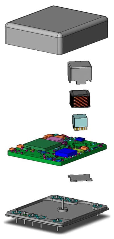
This latest clock has been jointly developed at Symmetricom, Draper Laboratory and Sandia National Laboratories in the US. The clock comprises a highly compact “physics package” that contains the caesium atoms used and sits on a circuit board within a tiny box. The caesium atoms are held within a resonance cell and are heated to a vapour state by plates situated at the top and bottom of the package.

Modulating microwaves

An optimized vertical-cavity surface-emitting laser (VCSEL) is shone through the vapour, causing excitation in the caesium atoms. The laser light is modulated by a microwave signal generator on the chip. This allows the laser’s single beam to excite the caesium atoms at two different energy levels. Interference between these two levels is then detected by a photodiode that forms part of a feedback loop. The loop optimizes the number of photons absorbed by the caesium atoms. The clock indicates that 1 s has elapsed after counting exactly 4596,315,885 cycles of the microwave oscillator signal.

The physics package is vacuum sealed and then covered by a layer of magnetic shielding, before being placed on the printed circuit board (PCB), which is then sealed so that it is airtight. The lid and base plate of the array both serve as a second layer of magnetic shielding.

All the components on the PCB are optimized for power efficiency at the smallest size possible. As a result, the circuitry around the physics package consumes about 95 mW, with the physics package itself consuming about 10 mW. Allowing for production faults, the CSAC has a total power consumption of only 115 mW, according to Steve Fossi, Symmetricom’s director of business development.

Idea born at NIST

In 2004 Physics World reported that John Kitching and his team at the US National Institute of Standards and Technology (NIST) in Boulder, Colorado, created what was then the most compact and portable chip-scale atomic clock. So what is different about this latest device? According to Kitching, this new product is essentially a commercial version of the work pioneered by his group at NIST between 2001 and 2005. “The Symmetricom collaboration also had an active research programme during that time that was funded in parallel with ours by the Defense Advanced Research Project Agency [DARPA].”

While the Symmetricom and NIST clocks are about the same size, the main advantage of this new clock is that the power required to run it is much less than any previous commercial atomic clock: 115 mW, compared with more than 1 W for all other atomic clocks. “This means it will open many new applications for precision timing, particularly those where only battery power is available,” says Kitching.

“Because few DARPA technologies make it to full industrial commercialization for dual-use applications, this is a very big deal,” says Gil Herrera, director of Sandia’s Microsystems and Engineering Sciences Application centre. “CSAC now is a product with a datasheet and a price.”

“The work between the three organizations was never ‘thrown over the wall’,” says Sandia manager Charles Sullivan, using an expression that has come to mean complete separation of effort. “There was tight integration from beginning to end of the project.”

Jamming roadside bombs

The clock could find a use in disabling improvised explosive devices (IED) or roadside bombs that are detonated wirelessly using everything from mobile phones to toy remote controls. Such bombs can be disabled using portable jammers that block all communications signals in the area. While this solves the immediate problem of the bomb, it also prevents friendly forces from using radio communications. The CSAC would provide the precise timing required to jam bomb-related communications while allowing friendly signals to get through.

The device could also be used in places where GPS timing signals are not available, for example in deep-sea diving, mining and seismic research. In particular, the clocks could be deployed in underwater sensors that rely on the precision timing of seismic signals for oil and gas exploration. In this case, the clocks on each sensor would need to be accurate, small and run on very low power so that the sensors could remain underwater for prolonged periods of time. The CSAC has only 10–20% of the power requirement of existing sensor clocks but is about a 100 times more accurate.

Fruit flies ‘swim’ through the air

Physicists studying the flight of the fruit fly have concluded that the tiny creature’s wing motions are much closer to the movement of swimming organisms than previously thought. This surprising result lends credence to the controversial suggestion put forward by some evolutionary biologists that flight could have evolved gradually from swimming as life left the oceans.

The wings of birds and insects are structurally quite similar to the fins and paddles of aquatic animals. However, flying and swimming seem to involve completely different physical processes. Flying organisms propel themselves using the lift forces generated as a wing slices through the air, while swimming organisms paddle forward using the viscous drag of water. As a result, some biologists have doubted that flight could have evolved from swimming.

Aeronautical inspiration

Flying creatures generate force (or lift) on their wings as they move through the air. Fruit flies remain airborne by sweeping their wings back and forth in the horizontal plane to generate lift. Propulsion can be achieved by tilting the angle of the wings with respect to the horizontal plane, thereby shifting some of the lift into the forward direction.

Drag hinders performance and as a result wings tend to be highly streamlined. But now a research team at Cornell University in New York has found evidence that fruit flies might also use viscous drag during flight.

Observing the wing motions of an insect is extremely difficult: a fruit fly flaps its wings 250 times per second. Using cameras recording 8000 frames per second, the team filmed fruit flies both hovering and in forward motion at various speeds. If the flies were propelling themselves purely by tilting their wings to shift the lift forward, the tilt should have increased as they flew faster. But the footage showed that, in some cases, the wings remained almost horizontal irrespective of flight speed.

However, the flies appeared to be adjusting the tilt of their wings in a more complicated manner. When they were hovering or flying slowly, the average angle of their wings was near-vertical, with the wing tilted in opposite directions on the forward and backwards strokes. Inevitably, the drag forces of the air on the wing also push the insect back and forth, but the two cancel each other out and overall the insect does not move far.

Maximizing drag

When they wanted to fly quickly, the fruit flies tilted their wings closer to the horizontal on the forward stroke to slice more cleanly through the air and then closer to the vertical on the backward stroke to maximize drag – effectively paddling through the air.

The team claims that this is the first indication of a flying organism deliberately manipulating drag forces to generate forward thrust. “These insects have a lot of drag forces acting on them and usually these forces cancel each other, but when the insect shifts its angle of attack a little, it is able to take advantage of them very rapidly,” explains group member Itai Cohen.

David Lentink of Wageningen University in Amsterdam and the California Institute of Technology, is impressed. However, Lentink, who was not involved in the research, does sound a note of caution. “It is difficult to say that all insects apply this mechanism, especially because, compared with some other insects, the fruit fly is more of a slow, forward hovering insect than a fast, agile forward flier,” he says. Cohen’s group is currently working on a comparative study across various creatures.

Cohen emphasizes that none of this proves that flying actually did evolve from swimming. “What we are showing with this work is that controlling your forward motion is basically the same regardless of what medium you are in, so at least that part of the jump would not have been that difficult,” he explains.

The research is described in Phys. Rev. Lett. 106 178103.

Translucent curtains soak up sound

Researchers in Switzerland have developed a new kind of lightweight curtain that can absorb sound waves while still letting light through. They say it is ideal for soaking up noise in offices, conference rooms or other places where natural light is needed.

Noise can be a major source of irritation at work or in the home, reducing productivity and making it hard to relax. Unfortunately, many of the materials used in interior design, such as glass and concrete, are what are known as acoustically hard. These materials reflect sound waves and so do not reduce levels of noise within a room.

On the other hand, acoustically soft, or porous, materials absorb a portion of the sound energy that strikes them. The fraction of energy absorbed depends on the frequency of the sound. Absorption occurs because air moving through such materials is slowed down by friction, which causes some of the sound energy to be converted into heat.

Lightweight and translucent

Usually, sound-absorbing materials are placed on the floor or ceiling, for example in the form of carpet or special kinds of tile. In places where the floor or ceiling cannot be modified, curtains can be used instead. But these are generally heavy and opaque. The new curtains, on the other hand, are lightweight and translucent.

The material for the curtains was designed using a computer model developed by researchers at Empa, the Swiss Federal Laboratories for Materials Science and Technology. The model was used to predict the acoustic behaviour of a variety of curtains, with properties such as a curtain’s size, porosity and mass per unit area altered to maximize sound absorption over a wide range of frequencies. Textile designer Annette Douglas then used the model to build an actual material – weaving together four or five different modified polyester yarns in such a way as to maintain the absorption characteristics while also ensuring fire resistance and light transmittance.

The material was then put to the test inside Empa’s reverberation chamber – a room in which sound waves are made to diffuse uniformly or randomly. With the curtain positioned 15 cm from a wall, the researchers found it could absorb up to five times as much sound as typical lightweight curtains. At low frequencies of about 200 Hz, it absorbed no more than about a fifth of the incident sound energy. However, at frequencies above 500 Hz (human ears having a maximum sensitivity between about 3000–4000 Hz) the material absorbed around three-quarters of the incident sound energy.

Astonished acousticians

“Acousticians are pretty astonished when they see the readings we are achieving with the new curtains,” says Kurt Eggenschwiler, head of Empa’s acoustics/noise-control division.

The curtains have been made into commercial products by silk weavers Weisbrod Zürrer and are now entering the German and Swiss markets. According to Douglas – whose company Annette Douglas Textiles sells the products – the curtains cost about 40% more than “a regular sheer fabric produced in Switzerland”.

Ken Gilbert of the National Center for Physical Acoustics at the University of Mississippi in the US thinks that the new curtain will “be well received and have a strong market”. He points out that sound-absorbing materials are generally used to reduce noise coming from objects within the room in question, whereas the new material will also be to reduce noise coming from outside through open windows. “This is an added bonus,” he says.

High-energy events in the Eternal City

By Edwin Cartlidge, Rome, Italy

Rome, the birthplace of nuclear physicist Enrico Fermi, is this week hosting a conference dedicated to discussing results from the NASA satellite that bears his name. Some 400 scientists have gathered in the Italian capital to discuss what the Fermi Gamma-Ray Space Telescope, launched in June 2008, can tell us about all manner of extreme celestial events – from the accretion of matter by supermassive black holes and ultra-energetic events known as gamma-ray bursts to the hypothesized collision of dark-matter particles.

First up on to the vast stage of the echoey Aula Magna at La Sapienza University was NASA’s Elizabeth Hays, who gave an overview of Fermi’s progress to date. Hays says she was happy to report that Fermi’s operations were “becoming almost mundane”, now that the satellite has been circling the Earth for over 1000 days, completing more than 16,000 orbits in that time, and collecting vast quantities of gamma-ray data in the process. (There is even now a Fermi app for the iPhone/iPad.)

Some of the gamma rays collected by Fermi have their origins on Earth, with Hays pointing out that radiation generated by charged particles during thunderstorms created something of a minor storm of their own on the Web with nearly half a million views of a NASA video explaining the process (see video above). Fermi’s principal source of gamma radiation is, however, outer space, and it surveys almost the whole sky in three hours, making increasingly detailed studies of bright sources and attempting to pinpoint the nature of weaker ones.

The first catalogue of distinct gamma-ray sources revealed by Fermi was released about a year ago and researchers have been working furiously to get a second, more precise catalogue published. As Dave Thompson of NASA’s Goddard Space Flight Center explained, this has taken a lot longer to produce than expected but he argues that when it comes out later on this month it will represent a “major revision” of the old catalogue, listing some 1888 active galactic nuclei and other gamma-ray sources.

Many of those who have made the trip to Rome will also be hoping that another high-profile – and very expensive – astroparticle mission will finally get to make the trip into space in the next few days or weeks. That mission is the cosmic-ray observatory known as the Alpha Magnetic Spectrometer, which is expected to launch on 16 May on the space shuttle Endeavour. As speaker Giovanni Bignami of the University of Pavia put it, “we are keeping our fingers crossed”.

Willard Boyle: 1924–2011

Willard Boyle, who shared the 2009 Nobel Prize for Physics, has died at the age of 86. Boyle was awarded one half of the prize with George Smith for inventing the charge-coupled device (CCD) camera. Boyle and Smith were both working at Bell Laboratories in New Jersey when they made their discovery in 1969 – Boyle was director of device development at the lab and was Smith’s boss; Smith was a department head. The other half of the 2009 prize went to Charles Kao for his work on optical fibres.

Boyle was born in Amherst, Nova Scotia, on 19 August 1924. His family moved to a remote logging community in Quebec, where Boyle was home-schooled by his mother until the age of 14. After serving in the Royal Canadian Navy in the Second World War, he then attended McGill University, receiving a PhD in physics in 1950. Boyle joined Bell Labs in 1953, where he spent the rest of his career before retiring in 1979 and returning to his native Nova Scotia.

Like many Nobel laureates, the prize came late in Boyle’s life, when he was 85. As his long-time friend and Nova Scotia local councillor Ron MacNutt told the Canadian Broadcasting Corporation yesterday, Boyle “had some regret that that recognition came a little bit late for him to get out and do more of that, to talk to younger children in school”. An earlier award, MacNutt added, might have let Boyle influence even more people in his life.

Revolutionary pioneer

The invention of the CCD revolutionized photography because the devices allow images to be converted directly into digital data rather than using film. CCDs once formed the basis of all digital cameras, but have since been replaced by CMOS sensors in most low-cost applications such as mobile phones and some digital cameras. CCDs are also widely used in astronomy, with the Hubble Space Telescope, for example, having several CCD cameras on board, including in the Wide Field Camera, which was recently upgraded.

A CCD camera contains millions of light-sensitive cells that are arranged in rows and columns to form a matrix. Incoming light is converted via the photoelectric effect into an electron, which is stored in a capacitor, with the amount of stored charge in each cell being proportional to the intensity of light. The charges are then transported to the edge of the CCD matrix to be read out, allowing the image to be reconstructed from the contents of each pixel.

Boyle was made a Companion of the Order of Canada in 2010 and received several other awards for his CCD work – including the IEEE’s Morris N Liebmann Memorial Award, which he shared with Smith. He is survived by his wife Betty and three children.

Nanotech industry comes under fire

A UK researcher is calling into question the capability of the nanotech industry to turn fundamental research into robust technologies that can be produced on a large scale. Mike Kelly at the University of Cambridge argues that manufacturing constraints will prevent structures smaller than 3 nm in size from being mass-produced using “top-down” processes.

“There are many billions of dollars being spent on one-offs while the bull in the china shop is the ultimate challenge of manufacturability,” Kelly told physicsworld.com.

Kelly is making these claims after carrying out a case study of the production of vertical nanopillars, which have been touted for uses in sensors and displays. These components can be produced at present by two different top-down approaches: using a metal particle catalyst to grow the pillars; or by infilling holes in a resist layer that can be defined using lithography.

Intolerable variations

Kelly considered the variability in the properties of nanopillars created using these two production methods and found that a large standard deviation in size and shape started to creep in once the scale reached below 3 nm. This, he says, would lead to intolerable variations in their electronic, optical and other properties if the nanopillars were to be used in applications.

On the back of his findings, Kelly believes that, given specific tools for fabrication, some nanostructures are intrinsically unmanufacturable. “The statistics of small numbers means that currently used methods will simply produce artefacts with too big a variation between adjacent features to be useful for anything,” he said. “If I am wrong, and a counter-example to my theorem is provided, many scientists would be more secure in their continued working, and that is good for science.”

‘Perfect’ structures

Rod Ruoff, a materials scientist at the University of Texas at Austin, agrees that some nanostructures below certain sizes will not be sufficiently stable in their structures and chemistries for all applications. “It is thus valuable to raise questions about what length scales are realistic, for each technology, for each application,” he said.

But Ruoff disagrees that bottom-up processes cannot be used to produce consistent specifications in bulk, and he highlights carbon as a promising material. “One of the attractive features of carbon nanotubes and graphene is their relative chemical stability, and the fact that such nanostructures can in fact be ‘perfect’ in structure even at the Angstrom length scales.”

Order from disorder

This is a view shared by Philip Moriarty a nanomaterials researcher at the University of Nottingham in the UK, who says that the limitations of top-down fabrication are already well-recognized by academics and industrial scientists. “This has prompted an intense research effort focussed on exploiting so-called bottom-up techniques such as self-assembly and, in particular, directed self-assembly.”

By this, Moriarty is referring to processes in which disordered systems of components form organized structures as a consequence of specific, local interactions among the components. This directed self-assembly is described by some as a hybrid of top-down and bottom-up fabrication techniques.

Moriarty believes that Kelly has presented the “effective error bars” associated with nanofabrication, rather than a general theory. He also said that he disagrees fundamentally with the assertion that scientific research should be focused on what can be manufactured now. “Fundamental nano scientific research should not be constrained by our current understanding of the limits of nanomanufacturability.”

This research is described in the journal Nanotechnology.

Nano-antenna fashions charge from light

A new device that collects and focuses light before converting it into a current of electrons has been developed by researchers at Rice University in the US. The nano-optical antenna and photodiode – the first device of its kind – could potentially be used in a variety of applications such as photosensing, energy harvesting and imaging.

Conventional antennas, which are widely used to transmit radio or TV signals, can be used at optical frequencies as long as the device is shrunk to the nanoscale. Such optical nano-antennas work by exploiting “plasmonic modes”, which increase the coupling between light emitted by neighbouring molecules and the antenna.

Naomi Halas and colleagues have now taken advantage of these plasmonic modes to make the first optical nano-antenna that also works as a photodiode – a type of photodetector capable of converting light into either current or voltage. Halas’s team made its device by growing rod-like arrays of gold nano-antennas directly onto a silicon surface – so creating a metal–semiconductor (or Schottky) barrier formed at the antenna–semiconductor interface.

When light hits the antenna, it excites oscillating waves of electrons, known as surface plasmons (so-called because they travel near the surface of the metal). These energetic or “hot” electrons are then injected into the semiconductor over the Schottky barrier, thus creating a detectable photocurrent without the need for an applied voltage.

The resonators made by the researchers, who report their work in Science, have heights and widths of 30 nm and 50 nm, respectively, and are between 110 nm and 158 nm long. Each 15 × 20 array consists of 300 devices with a spacing of 250 nm between the antennas. The structure is surrounded by an insulating later of silicon dioxide and the ensemble is then electrically connected through an electrode made of indium tin oxide.

Applications galore

One advantage of the device is that the photocurrent generated is no longer limited to photons with energies above the band gap of the semiconductor, but instead to photon energies above the height of the Schottky barrier. The device can thus detect light below the band gap of the semiconductor, and at room temperature to boot. “The result is important because it enables a new way to capture and detect infrared photons using cost-effective, sustainable semiconductor materials such as silicon,” Halas told physicsworld.com.

The range of potential applications for this device is extremely diverse Naomi Halas, Rice University

As the plasmon resonance wavelengths in the device are in the near-infrared part of the electromagnetic spectrum, with shorter nanorods giving shorter resonance wavelengths, applications for the device could include silicon-based solar cells that would work in the infrared as well as in the visible parts of the spectrum. The fact that the devices work in the broad-infrared also means that they could be used to make low-cost silicon infrared-imaging detectors that might replace costly indium-gallium-arsenide detectors that work in the same spectral range.

“The range of potential applications for this device is extremely diverse,” says Halas. “For example, as it is capable of detecting sub-band-gap photons, it could find widespread use in on-chip silicon photonics that would no longer need to integrate additional semiconductor materials as detectors into chip designs – something that would also lower fabrication costs.” Halas adds that such nano-antennas could also be used in “unforeseen applications”, such as photosensing, energy harvesting, imaging and light-detection technologies.

Copyright © 2026 by IOP Publishing Ltd and individual contributors