Quantum dots boost solar cell efficiencies

Scientists in the UK and US have shown how to increase photovoltaic efficiencies by attaching nanocrystal quantum dots to patterned semiconductor layers. The approach exploits the phenomenon of non-radiative energy transfer and could, say the researchers, lead to a new generation of more efficient solar cells.

Semiconductor solar cells work by using the energy of incoming photons to raise electrons from the semiconductor’s valence band to its conduction band. A potential barrier formed at the junction between p-type and n-type regions of the semiconductor forces the pairs to split up, thereby producing a current.

A solar cell’s performance is measured by its efficiency; in other words how much electrical power it generates for a given incident solar power. Cells consisting of a single p–n junction that are made from bulk semiconductor have a maximum theoretical efficiency of 31% — and the best performing affordable commercial devices are about 18% efficient.

Carrier multiplication

One way in which scientists are trying to overcome this limit is to make cells from billions of tiny pieces of semiconductor known as quantum dots, rather than one large piece of semiconductor, because these can harness light more effectively and can also create multiple carriers from each incoming photon — a process known as “carrier multiplication”.

Unfortunately, carriers in quantum dots are not as mobile as in bulk semiconductors and are usually trapped in crystal impurities. In addition, immobile carriers are attracted by neighbouring carriers of opposite charge and by coupling together they annihilate and emit a photon in exactly the reverse process that created the carriers in the first place.

Pavlos Lagoudakis of Southampton University and colleagues say that they can overcome these problems by combining the light-absorption ability of quantum dots with the current-generating capacity of a bulk semiconductor.

To demonstrate this they etched an array of rectangular channels some 500 nm wide into a layered semiconductor structure. The structure comprised a multiple-quantum-well (MQW) layer sandwiched between a p-type layer and an n-type layer. The MQW itself comprised 20 layers of gallium arsenide, each about 7.5 nm thick.

They then deposited a solution of cadmium-selenium quantum dots, each just a few nanometres across, onto the structure.

Inspired by photosynthesis

The idea, says Lagoudakis, is to take advantage of the “non-radiative energy transfer” used in photosynthesis. The photo-generated carriers within the quantum dots, which are confined within the etched channels, are close enough to the quantum wells that they can exchange energy via a dipole–dipole interaction. “Appropriate engineering of the hybrid device allows for the coupling of the electronic properties of the different components in a way that we get the best properties from each system,” he adds.

To prove that their device was enhancing current output via non-radiative transfer, the researchers also deposited quantum dots onto a substrate without channels. They reasoned that this unpatterned device would not support non-radiative transfer because the photo-generated carriers would be too far apart to interact via dipole–dipole interaction, and that it would therefore produce a much smaller current for a given light input than the patterned device. This is what they found: the patterned device, they report, was six times more efficient than the unpatterned one.

Lagoudakis and colleagues are now designing devices that can combine this feature of non-radiative energy transfer with carrier multiplication by appropriate engineering of the p–n junction and choice of materials for the quantum dots. Such devices, he believes, will exceed the 31% efficiency limit. He admits that these devices would cost more than existing silicon solar cells because the “molecular beam epitaxy” technique used to make the layered structure is expensive. However, he maintains that because the biggest cost in manufacturing solar cells is in fact associated with housing the device, an improvement in efficiency, which would reduce the “active area” of the device, could lead to cheaper solar cells overall.

Thinner and cheaper?

Solar cell developer Martin Green of the University of New South Wales in Australia believes that the research by Lagoudakis’ team is interesting because cells made from quantum dots may prove to be thinner and cheaper than traditional cells. But he cautions that the group may not have chosen the ideal reference device to demonstrate increased photocurrent. He says it would have been better to have used as a reference an identical device but with no quantum dots attached as this should also be more efficient than the unpatterned device.

Father figure

darwin+1.jpg
Leonard Susskind: a Darwinian physicist

By Matin Durrani

He probably won’t like me for saying this, but Leonard Susskind of Stanford University looks a bit like Charles Darwin.

The reason I know is that Susskind – one of the father figures of string theory – flashed up a slide of the great man (Darwin that is) during a public lecture last night held as part of the University of Bristol’s centenary celebrations and the city’s Festival of Ideas.

It was uncanny: Susskind’s grey beard and thinning hair make him a dead ringer for Darwin, who was born 200 years ago this year. I wonder if anyone’s told him of the likeness before?

Attended by nearly 700 people packed into the university’s neo-gothic Wills Memorial Building, Susskind’s lecture was entitled “Darwin and the cosmic landscape”, in which he examined Darwin’s influence on physics.

Susskind’s thesis is that by putting forward the then radical idea of a natural explanation of the origins of life, Darwin “set the standard for what an explanation should be like”. In other words, as Susskind eloquently explained, by rejecting the idea that life was too improbable too have arrived by accident and that there must be some sort of grand designer, Darwin instead sought a scientific explanation for the existence of life.

As Susskind pointed out, there are four different base pairs on a DNA molecule (A, G, C and T) and with each molecule having typically 10^8^ base pairs, there must be 4 to the power 10^8^ different ways of arranging those base pairs. Genetic mutations allow different arrangements, which – eventually – leads to the “tree of life”.

But what’s all this got to do with physics? Well, string theory permits the existence of a “landscape” of about 10^500^ different universes. We live on one of these universes – the one that permits the existence of life. It’s essentially an anthropic argument – the world is fine-tuned so we’re here to observe it.

I won’t go into the details here, but you can find all you need to know about this subject in an article by former Physics World features editor Matthew Chalmers, who also rolled up at last night’s lecture and was one of several people to pop Susskind a question.

(more…)

Einstein and Old Harry

By Hamish Johnston

I have just heard what has to be the longest string of physics jokes ever uttered on the radio.

I was listening to the BBC Radio 4 programme “Old Harry’s Game”, in which the comedian Andy Hamilton plays Satan and is set in hell.

Early in the episode we learn that Einstein is detained at Old Harry’s pleasure — indeed all deceased scientists are there it seems.

What follows is a string of gags on everything from Schroedinger’s Cat to Heisenberg’s uncertainty principle — and a joke of dubious taste about Stephen Hawking’s ability to play table tennis.

You can listen to it here — the physics jokes start about ten minutes in.

CULTURAL WARNING: Like most early-evening broadcasts on Radio 4 this programme could be a bit too “jolly-hockeysticks” for the non-British listener.

Microscope sees the Fermi surface

Scanning tunnelling microscopes (STMs) have been used for nearly three decades to study the surfaces of metals and semiconductors. But now physicists in Germany have discovered that the instruments can be used to measure the behaviour of electrons relatively deep within a material.

According to the researchers, the technique offers a completely new way of measuring the shape of the “Fermi surface” — the boundary between occupied and unoccupied electron energy states that defines many of properties of metals and semiconductors. And because STM can be sensitive to the spin of electrons, the technique could be used to characterize the tiny magnetic structures used in data storage devices.

An STM works by placing an extremely small metal tip (with just one atom at its point) very close the surface of interest. When a voltage is applied between tip and sample, electrons tunnel into or out of the material. The size of the tunnelling current is related to the surface properties of the material, such as mapping the locations of individual atoms.

Alexander Weismann and colleagues at the University of Goettingen, the Institute for Solid State Research in Juelich and the Martin Luther University in Halle made their discovery while developing an STM technique for locating atomic impurities below the surfaces of materials (Science 323 1190).

Colliding wavefronts

This involved studying samples of copper that contained minute quantities of cobalt. Electrons injected from the STM tip into pure copper should travel in wavefronts much like the ripples formed by a stone dropped in water. However, if such ripples encounter a cobalt atom they can be scattered back to the surface where they interfere to form a pattern that could be detected by the STM.

While the technique was able to locate the cobalt atoms, the team was surprised to see that the interference pattern was more complicated than expected from simple ripples. Instead, the pattern corresponded to the underlying symmetry of the copper crystalline lattice. The reason, according to the team, is that the ripples are being focused along certain directions in the copper — an effect that is defined by the shape of the Fermi surface.

Team member Martin Wenderoth at Goettingen told physicsworld.com that the technique is sensitive to the shape of the entire Fermi surface. By contrast, established techniques for measuring the Fermi surface, like electron cyclotron resonance and angle-resolved photoemission, map out only selected parts of it.

Wenderoth says that the technique could be used study local variations in the shape of the Fermi surface. For example, it could be used to study hidden interfaces in nanometre-sized multilayered structures.

Two Fermi surfaces

In particular, it could be very useful in characterizing layered magnetic structures such as those used in giant magnetoresistance (GMR) read heads for computer hard drives. This is because magnetic materials such as iron and cobalt have two different Fermi surfaces — one for spin up electrons and one for spin down electrons.

Spin-polarized STM, which is sensitive to the spin of the tunnelling electrons, would see two interference patterns if the electrons travelled through a magnetic layer — one for spin up electrons and the other for spin down. By observing the two different patterns, researchers could gain insight into the magnetic and structural properties of magnetic layers buried under a surface.

Do you have an eye for entanglement?

Experiments that reveal the weirdness of the quantum world usually involve precise and highly specialized equipment. But now physicists in Switzerland and the UK have proposed a way of using human vision to observe the purely quantum effect of “entanglement”.

The experiment — which has yet to be performed in the lab — would involve entangling a pair of photons and then creating thousands of identical copies of one of the pair such that they could be seen by the human eye.

Entangled particles have a much stronger relationship than that allowed by classical mechanics. For example, the polarization of one photon is revealed instantly by measuring the polarization its entangled partner, regardless of the distance between the photons.

The new experiment, which has been proposed by Nicolas Gisin and colleagues at the University of Geneva and University of Bristol, would first involve creating a pair of entangled photons. This could be done, for example, by passing light through a non-linear crystal in which a higher-energy photon is absorbed followed by the emission of two lower-energy photons (arXiv:0902.2896).

Cloning photons

One of the photons is then “cloned” to create thousands of identical photons. This is done by stimulated emission — the same process behind a laser — whereby the original photon is sent through a pumped optical medium.

Because the clones are created in a coherent quantum process, it produces a pulse of light that is intense enough to be seen with the naked eye — yet is entangled with the second original photon. Measuring the polarization of the pulse will therefore reveal the polarization of the second photon.

The team proposes to measure the polarization of the pulse by passing it through a polarizing filter, which allows light with parallel polarization to pass through while deflecting light with perpendicular polarization by 90°. Two human observers — one looking along the parallel path and the other the perpendicular path — could then determine the polarization of each pulse.

Meanwhile, the polarization of the second photon of the pair would be determined by passing it through a similar polarizing filter that is monitored by two sensitive photon detectors.

Predicting the outcome

If the experiment is a success, the humans should be able to predict the outcome of the measurement on the second photon based on the observed polarization of the pulse. In other words, if the pulse is vertically polarized, then the second photon will be horizontally polarized.

While entanglement in photons was first observed over 30 years ago, Gisin is keen to point out an important distinction between this and previous experiments. In earlier work, the choice of measurement that forces the entangled pair into distinct polarization states is made before that state is amplified to a level where it can be perceived by a human observer. For example, a single photon is passed through a polarizing filter and then converted into an amplified electrical pulse by a detector.

By contrast, in this experiment the entangled state is amplified to the human level before the measurement is made — effectively bringing the observer one step closer to the weird world of quantum mechanics. Indeed, Gisin believes that, if successful, the experiment could be extended to clone the second entangled photon and use a total of four human observers to verify entanglement.

‘Elegant experiment’

Seth Lloyd at the Massachusetts Institute of Technology told physicsworld.com that the proposal “does a considerable service by devising an elegant experiment where the human eye functions in a very efficient way as an entanglement detector”. However, he also points out that the eye is an extremely efficient detector of light, so it is not surprising that is could be used to detect entanglement.

Indeed, the challenges involved in actually doing the experiment are mostly related to the cloning process, according to Gisin. “Cloning cannot be perfect”, he explained, adding that unwanted spontaneous emission during cloning would create a significant number of photons that were not entangled.

This problem could be reduced using a technique called “phase covariant” cloning, but not eliminated. As a result, the experiment would have to be repeated many times over before the observers see enough entangled pulses to verify the effect.

Another challenge, according to Gisin, is producing cloned pulses of green light, which the eye is most sensitive to. Most cloning systems currently produce photons in the infrared.

“First we plan to amplify the photon so it can be seen”, said Gisin. “The rest should be relatively easy.”

Nanoscale friction: thinking big helps

Physicists should “think big” when it comes to calculating the effects of friction on tiny nanomachines, according to researchers in the US, who say that they have strong evidence against the widely held belief that friction at the nanometre scale is different than friction in the everyday world.

Friction can be a big problem for small objects. Nanosized devices have very high surface-to-volume ratios, which means that their surfaces quickly wear out or even spontaneously stick together as they come into contact. To be able to control friction at the nanoscale, scientists have to first understand where friction comes from.

Current models of nanoscale friction assume that nanoscale surfaces are perfectly smooth, when in fact they are rough — rather like a mountain range, where peaks correspond to individual atoms or molecules. While physicists can use continuum mechanics to deal with the roughness of large objects, roughness on the nanoscale is tricky because it is not clear how individual atoms and molecules would interact with a sliding surface.

Collection of atoms

Now, Izabela Szlufarska and colleagues at the University of Wisconsin, Madison, have performed computer simulations that look at nanoscale materials as a collection of atoms (Nature 457 1116).

The researchers monitor the positions and interactions of the atoms as the materials slide across each other. This is the first time that atomistic simulations of sliding friction have shown quantitative agreement with experiments carried out on the same material systems — sliding diamond-like carbon atomic-force-microscope tips on hydrogen-terminated diamond surfaces, says Szlufarska.

Our discovery provides a new and simple framework for interpreting nanoscale friction experiments Izabela Szlufarska, University of Wisconsin, Madison

The team discovered that the force of friction is proportional to the number of atoms that interact between two nanoscale surfaces. This is much like friction between larger rough objects, where the friction is proportional to the total area of interaction between two surfaces.

“Our discovery provides a new and simple framework for interpreting nanoscale friction experiments, which up to now had been interpreted by continuum mechanics models,” Szlufarska said. “And, our demonstration that roughness theories also apply at the nanoscale provides a foundation for building unified friction laws across all length scales.”

The researchers would ultimately like to use their simulations to build quantitative theories of friction that would allow them to predict the coefficient of friction for given materials and experimental conditions.

Desert mechanics

Giant sand dunes can gather into some of the most awe-inspiring patterns in nature. However, the mechanics of their formation has long remained a mystery. Now a group of physicists based in Algeria, the US and France suggests that the topology of these desert landscapes is governed by the thickness of the atmospheric layer above; a process similar to dunes forming on a river bed. The finding could act as a starting point for modelling the long-term evolution of desert environments, say the researchers.

After an expedition to the Algerian erg (a “sand sea”), the researchers combined field measurements with aerodynamic calculations to model the interaction between the desert floor and the atmosphere. They discovered that there exists a correlation between the separation of dunes and the height of the overlying atmospheric boundary layer — the part of the atmosphere that interacts directly with the Earth’s surface (Nature 457 1120).

“This study is fundamental: in principle our findings apply to all sandy deserts where the amount of sand available for transport by the wind is sufficiently large,” said Philippe Claudin, one of the researchers at the Laboratoire de Physique et Mecanique in Paris.

Learning from the river

The calming sight of evenly spaced dunes along a river bed is in fact the result of rough bed topography. Inconsistencies in the river bed cause turbulence in the water — leading surface waves — which in turn stabilize the water flow along the river bed. The result is a controlled repetition of “waves” in the river silt where the wavelength is directly proportional to the depth of the river.

According to Claudin and his colleagues, calculations reveal a similar process takes place in desert environments. Here, instead of a river surface, it is the ABL that acts as a stabilizer for “waves” in the desert — the thicker the ABL the larger the distance between neighbouring giant dunes.

Comparing dune separation from deserts around the world with the overlying ABL thickness, the researchers explained the range of mean spacing of 300 m in coastal terrestrial desserts to 3.5 km inland. Also, contrary to previous theories, the researchers report that giant dunes do not grow in a steady manner but result from the non-linear interaction of small dunes.

A complete picture?

“This study does a lot to convince that the overall stabilizing influence of the free atmosphere plays indeed a central role for limiting the size of giant dunes,” said Eric Partelli, a sand dune researcher at the University of Stuttgart.

Other researchers were less certain of the completeness of this theory. “The proposed mechanism is very appealing, but I think they could now calculate the time evolution and compare the final shape of the dunes with real world measurements,” said Hans Herrmann a researcher of Granular Matter at the University of Zurich.

Claudin told physicsworld.com that his team now plans to investigate specific dune fields in more detail. “We will start to look at dunes of all scales in order to go beyond the scale issue.”

Saw-toothed sapphire helps build polymer arrays

Producing ultra-dense, orderly arrays of nanometre-sized elements for next-generation electronic devices is no easy task, but researchers in the US have come up with a new way of tackling the problem.

Their technique involves placing a thin film of block copolymers onto the surface of a commercially available sapphire wafer. The process produces large films of highly patterned and densely packed nanostructures that are almost defect free (Science 323 1030).

The technique could lead to dramatic improvements in the data-storage capacity of electronic media, say Tom Russell at the University of Massachusetts Amherst, Ting Xu at the University of California Berkeley and colleagues.

The new work relies on the fact that molecules in thin films of block copolymers — two or more chemically dissimilar polymer chains linked together — will self-assemble into ordered patterns when spread out on a surface.

The problem in the past however, was that the order broke down as the area increased. This lack of order means that you can no longer write to or read individual domains, which means that such patterns cannot be used in data storage devices.

Saw-toothed ridges

Russell, Xu and colleagues have overcome this problem by layering the film of copolymers onto the surface of a commercially available “miscut” sapphire crystal — a crystal cut at a small angle to an atomic plane. When this crystal is heated to between 1300 and 1500 °C for 24 hours, its surface reorganizes into a highly ordered patterned of saw-toothed ridges that can then be used to guide the self-assembly of the block copolymers.

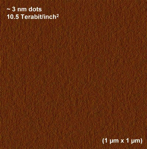
Using their technique, the researchers succeed in making almost defect-free arrays, measuring more than 3 × 3 cm2, that contain individual elements with feature sizes as small as 3 nm. This translates into a potential data-storage density of about 10 terabits per square inch. By contrast, the best commercial hard drives can store information at densities of about 200 gigabits per square inch, which is about one fiftieth the density achieved by the new technique.

Although sapphire was used in this work, Russell and Xu explain that other single-crystalline off-the-shelf materials, like silicon, can be employed to guide self-assembly too.

The technique is also better than using “top down” methods of nanopatterning, such as nano-photolithography, which is expensive, environmentally unfriendly (it uses harsh chemicals) and rapidly approaching the resolution limits of light.

The researchers have filed a joint patent on the technology.

NASA’s carbon-dioxide mission fails

NASA’s first mission to measure carbon dioxide (CO2) levels in the atmosphere has failed shortly after take-off earlier today. Officials said that the $270m Orbiting Carbon Observatory (OCO) did not reach orbit and landed in the Pacific Ocean near Antarctica.

The OCO was launched at 09:55 GMT on a Taurus rocket from the Vandenberg Air Force Base, California. However, 14 minutes after the launch, the Taurus rocket malfunctioned and the “fairing” — the part of the rocket that covers the satellite on top of the rocket — had failed to separate properly after launch so the satellite could not drift away in orbit.

The OCO was meant to orbit the Earth at an altitude of 705 km and produce “concentration” maps of carbon sources and sink throughout the world. The OCO would have provided samples of CO2 levels at around 34,000 locations as it orbited Earth once every 100 minutes.

As sunlight is reflected from the Earth’s surface, gases such as CO2 and oxygen absorb this light at specific wavelengths. The OCO was launched with three spectrometers tuned to detect changes in the intensity of this absorption.

The OCO was to be the sixth satellite to join the “A-train” — a set of seven Earth-observing satellites — which includes the CALIPSO and Cloudsat satellites looking at the levels of aerosols in the Earth’s atmosphere and monitoring cloud formation that were both launched in April 2006.

In January, the Japanese space agency, JAXA, launched the world’s first satellite dedicated to monitoring greenhouse gas emissions. Named Ibuki, which means breath in Japanese, the satellite orbits 667 km above the Earth’s surface and has the sensitivity to detect changes in CO2 levels by around one part per million, which Ibuki will measure at 56,000 locations on the globe.

Chasing the Green Comet

comet.jpg
Comet Lulin photographed on 31 January, 2009. Courtesy Joseph Brimacombe, Cairns, Australia

By Hamish Johnston

If you are blessed with clear skies tonight you might want to look to the heavens and see if you can spot the Green Comet — aka Lulin.

Today, the comet will be the nearest it gets to Earth and if you are very lucky you could see it with the naked eye. And if you use binoculars, you have an even better chance of spotting the object — at least according to Sky & Telescope magazine, which has a helpful page on its website that points you in the right direction.

Happy comet spotting…

Copyright © 2026 by IOP Publishing Ltd and individual contributors