Rethinking MRI scans

Biomedical engineers in Switzerland have discovered a new way of using magnetic resonance imaging (MRI) scanners to produce images with more uniform quality. This technique could also remove the need for patients to be placed in a narrow tube, making the experience less intimidating, especially for children.

In a standard MRI scan, a magnetic field is applied to a body, causing the magnetic moments of hydrogen atoms to align. Following this, a radio frequency is targeted at the area to be imaged, knocking the moments out of alignment. As the hydrogen atoms relax they emit radio waves and these can be mapped to form images of the interior of the body.

Since the first MRI scan produced a blurry image of a human body in 1977, the machinery has been refined to produce high-quality medical images, particularly of soft tissues that are not well depicted in X-rays. However, an unpleasant aspect of the process is that radio wave interaction has to take place at close quarters with the patient; this is on account of the short range of standing radio waves.

Now, in a radical rethink of the process, a team led by David Brunner of the University of Zurich has demonstrated a new way of manipulating hydrogen atoms to produce images by using travelling radio waves sent and received by an antenna. Operators will now be able to produce clearer images over larger areas of the body, and the new technique would free up space around the patient, say the researchers.

Long range MRI

Brunner and his colleagues have scrapped the radio coils of classic MRI scanners and replaced them with a waveguide and remote antenna. Apart from this, their MRI technique remains unchanged from the classic process. Essentially, they have replaced a standing radio wave interaction with travelling radio wave interaction, which has a range of metres.

We had hit a bit of a wall with using higher fields so this has now broken open the ceiling for obtaining higher quality images. Philip Grandinetti, Ohio State University

In their demonstration, Brunner and his team placed the cylindrical waveguide into a 7 Tesla scanner and placed an antenna at one of the ends. They used this arrangement to generate images of the lower leg of a human volunteer. Reporting their results in Nature (457.07752), they compare their images with those from a traditional scan and show a much improved resolution.

According to the researchers this amendment to the traditional MRI scan would not require any alteration to existing equipment beyond the introduction of a waveguide and antenna. “The technology is quite simple and in some ways actually simpler than the existing solutions. It is also arguably safer because the transmitter is further removed from the patient,” said Klauss Pruessmann, one of the researchers at the University of Zurich.

Policy hurdles

Philip Grandinetti, an MRI researcher at Ohio State University, told physicsworld.com, “In theory, hospital implementation could be almost immediate. We had hit a bit of a wall with using higher fields so this has now broken open the ceiling for obtaining higher quality images.”

Within the European Union, a hindrance may come from the legislation of 2004 set to restrict occupational exposure to electromagnetic fields. After being met with considerable protest by the MRI community, implementation of the MRI and Physical Agents (EMF) Directive has been postponed until 2012 to allow a more amicable solution to be sought. But given the 7 Tesla fields required by this new technique, compared with the 3 Tesla of ‘standard’ machines, adoption of this new technique could face political barriers.

“We will use travelling-wave approach for uniform coverage of large volumes, such as the entire head, for neuroscientific studies. We will also investigate the combination of travelling-wave excitation with close-range array detection, which would combine uniform and safe excitation with sensitivity benefits of array detection,” Pruessmann told physicsworld.com.
New technique to tackle nuclear waste

Physicists at the University of Texas have proposed a new type of fusion reactor that could destroy the most biologically hazardous nuclear waste. It would consist of a spherical tokamak containing a deuterium-tritium plasma, which would produce streams of neutrons that would be fired into the waste held in a “blanket” around the reactor. If built, the reactor could be operational in 15–20 years’ time and could even be used to generate electricity.

High-level nuclear waste contains not only uranium and plutonium but also other “transuranic” elements that are heavier than uranium and are the principal source of longer-lived radiation. Most such waste is put into stainless-steel flasks and stored in vaults, although it is possible to reprocess spent fuel and separate uranium and plutonium from the fission products. Some countries, like the US and Finland, are even planning to store unprocessed spent fuel for hundreds of years in costly underground repositories.

The new reactor, proposed by Mike Kotschenreuther, Prashant Valanju, Swadesh Mahajan and Erich Schneider would destroy the transuranic waste in a two-step process both involving the process of “transmutation”. The idea of transmutation has been around for some time and involves converting radioactive material, with a half-life on a geological timescale, into something with a much shorter half-life. Waste would still need to be stored, but its long-term hazard would be reduced.

However, existing transmutation methods, which are based on fission alone, cannot deal with transuranic elements. What the Texas team is proposing is to first attack the waste by placing it in a standard nuclear plant such as a light water reactor (LWR), which would destroy almost 75% of the transuranic waste by transmutation. The rest — non-fissile transuranic elements such as plutonium-242, americium-243 and curium-246 that cannot be destroyed by LWRs because the flux of neutrons is not high enough — would be destroyed by neutrons from the new reactor.

Kotschenreuther and colleagues’ proposed Compact Fusion Neutron Source (CFNS) is a version of the Mega Amp Spherical Tokamak (MAST) reactor at the UK Atomic Energy Authority in the UK and the National Spherical Torus Experiment (NSTX) at Princeton University in the US. It would generate neutrons by fusing deuterium and tritium nuclei but the magnetic field would be about 7 T — much higher than in MAST or NSTX — to increase the fusion pressure and so create a high enough fusion flux. Transuranic waste would be destroyed by loading it around the CFNS’s core. The CFNS would also contain a new kind of divertor, which remove the heat from the sides of the reactor.

The researchers say that their reactor could also be used to generate power as the transuranic waste burns, with about 90% being potentially sold to the grid and the rest used to keep the fusion process going. The researchers say that only one such machine would be needed to destroy the transuranic waste from 15 LWRs. “Realistically, if funding is available, the CFNS could be ready in 10–20 years,” says Swadesh, who thinks that it could cost a tenth of the €10bn being used to build the ITER fusion experiment in France.

One big problem with the technique is that the reactor would have to operate continuously. Currently, MAST and NSTX operate fusion for only 10 s, with only the KSTAR tokamak in South Korea operating for 1000 s. “The idea is attractive,” says David Ireland, a nuclear physicist from the University of Glasgow in the UK. “But there are some technical issues that would first need to be overcome such as if it is possible to maintain the plasma for long durations.”

Nanoelectronics made easy

Physicists in the US and Germany have developed a new approach for making tiny structures that could someday be used in electronic devices.

The team has used the technique to fabricate transistors with features at sizes of just 2 nm — which they have dubbed “SketchFETs”. What’s more, the devices can be erased and reformed as desired, a result that could be important for nanoelectronics applications.

Most transistors today are made from silicon using optical lithography, but it is difficult to shrink these devices to below about 20 nm.

The new technique, developed by Jeremy Levy and colleagues at the University of Pittsburgh and University of Augsburg, can produce features that are 10 times smaller in linear terms and 100 times smaller in terms of area than devices at the end of the “roadmap” for commercial silicon devices, says Levy.

The technique, which was first described last year, involves using the probe of an atomic force microscope to sketch conducting paths, or wires, just a few nanometres across, at the interface of a crystal of strontium titanate and lanthanum aluminate (both of which are insulators).

Potential for memory devices

The wires can then be erased using a reverse voltage or with light, which renders the structure insulating again. It is the reversible nature of the process that makes it potentially useful for applications like memory devices, explains Levy.

Now, the team has taken its technique a step further by fabricating tiny field-effect transistors and tunnel junctions as well as just conducting wires on an insulating substrate (Science 323 1026). Because these devices measure just 2 nm across, many of them can be packed into a given area.

According to the researchers, this new route to nanoelectronics will be important for making high-density memories, chemical sensors and computer processors.

And that’s not all: because the devices approach the atomic scale, they can be used to study quantum mechanical phenomena such as tunnelling. Understanding such behaviour will be crucial for modelling novel electronic materials and perhaps even for making quantum computers in the future.

UK media meet astronomy

meridian.jpg
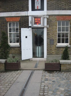
Greenwich Meridian – longitude zero since 1851

Last night, the Royal Observatory at Greenwich became a melting pot of science and journalism as it played host to the UK media launch of the International Year of Astronomy.

Key speakers included cosmologist and Royal Society President, Martin Rees; Observatory Director, Kevin Fewster, and the UK Chair of IYA2009, Ian Robson.

I arrived in early, while it was still daylight, to get the obligatory snap of me straddling the Greenwich Meridian, the prime meridian of the World (Longitude 0º) since the late 19th Century.

Highlights of the evening included an impressive tour in and around the solar system via the Peter Harrison Planetarium – Europe’s first digital laser planetarium projector; a Q&A session with the Public Astronomer, Marek Kukula; and astronomically themed music performed by students from the neighbouring college of music.

Unfortunately, the planned live link up with the Liverpool Telescope – confusingly housed in the Canary Islands – didn’t quite work out. Apparently, humidity in the Spanish archipelago was at 90 % so nothing could be seen through the veil of mist.

Star of the show was undoubtedly Rees, who delivered a pitch perfect history of astronomy and its cultural force over the past 400 years since Galileo first pointed his telescope to the skies.

The nice thing about his speech was its optimism. So often, in these times of environmental and economic turmoil, keynote speeches by eminent scientists can be doom laden with very few flickers of hope. While Rees checked the climate change box, he didn’t pitch the need for Government action as an end in itself; he waxed lyrical on the incentives for protecting the planet, in particular the sense of awe inspired by astronomy and how this can put global issues in perspective. Referring to the campaign for “dark skies” he said:

“It’s not just astronomers who care about this, just as its not just keen ornithologists who would feel deprived if song-birds disappeared from our parks and gardens”.

One particularly notable project in the UK IYA2009 programme is the Telescopes for Schools project which will see 1000 UK schools receive a free telescope over the next year. Picking up the bill is a combination of the Society for Popular Astronomy, the Royal Astronomical Society and the UK science-research funding body STFC.

I caught up with the project leader Helen Walker of the Rutherford Appleton Laboratory and she told me she had been putting the finishing touches to the accompanying DVD over Christmas and the telescopes are ready to be rolled out to schools over the next few months:

“The kids should get some great views of the Moon, with plenty of crater detail and they can hopefully get some sightings Jupiter and Saturn. We’re hoping schools will include telescopes in science lessons but also set up after school clubs to get the great views the darkness will bring.”

Jupiter pips Saturn for new space mission

NASA and the European Space Agency (ESA) have agreed to develop two co-ordinated scientific missions to study Jupiter and several of its moons. NASA’s Jupiter Europa Orbiter and ESA’s Jupiter Ganymede Orbiter are scheduled for separate 2020 launches and should reach the Jupiter system in 2026. The combined effort is called the Europa Jupiter System Mission.

Before the agreement, which was struck at a meeting in Washington last week, NASA had been considering two missions to the gas giants — one to Europa and the other to Saturn’s moon Titan. Likewise, ESA was looking at missions to Jupiter and Saturn, with the possibility of landing on Europa and Titan respectively. Officials from both agencies have now decided that it will be more feasible to implement a co-ordinated Jupiter mission first.

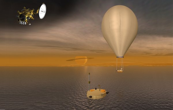
However, the Saturn mission has not been forgotten, with the two agencies planning to “move [it] forward for further study and implementation”. Dubbed Titan Saturn System Mission, the joint project is expected to consist of a NASA orbiter and an ESA lander and research balloon. It will be launched sometime after the Jupiter mission.

‘Win, win situation’

Ed Weiler of NASA’s Science Mission Directorate called the agreement a “win, win situation”, adding “a Saturn system mission clearly remains a priority for the science community”. David Southwood, ESA’s director of science and robotic exploration, described the joint endeavour as “a landmark of 21st century planetary exploration”.

The Europa Jupiter System Mission orbiters will spend at least three years studying Jupiter and its moons Callisto, Gannymede, Europa and Io. The Jupiter Europa Orbiter should shed further light on whether oceans of liquid water exist on Europa — and whether the moon could harbour life. Meanwhile, the Jupiter Ganymede Orbiter could help scientists to understand why Ganymede is the only moon in the solar system known to have an internally generated magnetic field. The two orbiters will also work together to gain a better understanding of the formation and evolution of the Jovian system.

NASA and ESA have already collaborated on planetary missions. In 1997 they launched the Cassini–Huygens joint mission to Saturn, in which NASA supplied the Cassini orbiter and ESA built the Huygens probe.

Detecting colour on the nanoscale

Scientists in the US have copied the way the retina sends electrical signals to the brain in order to construct nanoscale colour detectors. The devices, composed of carbon nanotubes decorated with photosensitive molecules, can detect very weak sources of visible light at specific wavelengths and could have applications in astronomy and biology.

The ability to detect photons over just a few square nanometres is useful in studying light sources that are either very weak or very small. To date, researchers have attempted this largely through the construction of solid-state devices, which produce electron-hole pairs when illuminated. However, building such devices with nanoscale precision is extremely difficult.

Xinjian Zhou and colleagues at the Sandia National Laboratories in California are taking an alternative approach, which is similar to the way that retinal molecules absorb light and then convert the light into electrical signals. This involves coupling light-sensitive molecules to transistors made from single-walled carbon nanotubes, rolled up sheets of graphite with a diameter of around 1 nm, and measuring the change in conductance of the nanotubes when the molecules absorb photons and change shape (arXiv:0902.2231).

Detector and amplifier side by side

As Zhou explains, this arrangement is able to detect extremely weak sources of light. ”We have a detector and a signal amplifier built next to each other in our system,” he says. “With the amplification effect from the nanotube transistor, we can reach high sensitivity.”

Other researchers have demonstrated this effect using a variety of photosensitive molecules, but until now have only been able to detect light outside the visible spectrum. Zhou’s group has extended the technique to visible wavelengths, and has shown how wavelengths within specific narrow bands can be detected.

Zhou and colleagues did this using “chromophores” — molecules that generate colour — based on the compound azobenzene (consisting of two rings of carbon and hydrogen atoms similar to benzene). To build their nanoscale detectors they attached carbon nanotubes to a 10 cm long silicon wafer, evaporated electrical contacts onto the wafer, and then immersed the wafer in a solution containing the chromophores, which then attached themselves to the nanotubes.

Sensitive to different wavelengths

They then illuminated individual nanotube devices, each comprising a portion of the wafer 2 µm long and 1 nm wide, with monochromatic light from across the visible spectrum and recorded the electrical signals generated by each of three types of chromophore (each sensitive to different wavelengths). They found that their nanodetectors were sensitive down to about 40 W/m2, about 3% of the density of sunshine reaching the ground.

By combining their experimental results with theoretical calculations, the Sandia group concluded that a change in the geometry of the chromophore molecules brought about by illumination alters the chromophores’ electric dipole moment, which in turn creates an electrostatic potential on the nearby nanotubes, effectively changing the gate voltage of the nanotubes and thereby regulating their conductivity.

According to Zhou, the work could provide important insights into basic science, by using nanotubes to study how individual molecules respond to light and change shape. He also says that, if they can be made to work at slightly longer wavelengths, their nanoscale optical sensors could be used as ultrasensitive infrared detectors on telescopes, in order to image distant objects. In addition, he believes that one day the devices might be used to sequence genes. A single strand of DNA laid across an array of nanoscale detectors could in principle, he says, be sequenced if each detector picks up the light from the florescence tag on an individual base.

Commercializing the nanoscale detectors, says Zhou, depends on overcoming the hurdle currently confronting many applications of nanotechnology — being able to assemble nanoscale objects over large areas in a controlled way. “Adding the chromophores to the nanotubes is not difficult, neither is the integration of electronic components for the signal detection,” he adds. “But if only we could have a perfect array of nanotubes with the desired properties.”

Evidence mounts for axion-like particles

Less than three weeks after physicists spotted a tentative signature for axions, another research group is claiming to have “the strongest evidence yet” of the hypothetical particles. The new evidence, which again appears in astrophysical data, puts more pressure on Earth-bound experiments to find a signal.

Axions were first proposed in the late 1970s to solve an issue in particle physics known as the strong-CP problem. If they exist they would be very light and interact very weakly with matter, but these properties have made them difficult to find. No experiment on Earth has yet discovered any evidence of the particles.

However, researchers have predicted that axions could help electromagnetic radiation travel from distant sources — such as the bright “active” nuclei of certain galaxies — and that this process could reveal their existence. Indeed, astrophysicists know that the high-energy photons generated by active galactic nuclei (AGN) should be unable to travel intergalactic distances because they are absorbed by the universe’s opaque background of microwave radiation — yet telescopes still detect them.

Earlier this month, a group led by Malcolm Fairbairn of King’s College, London, found statistical evidence hinting that axions are the reason why we can detect the high-energy photons. The evidence suggested that the photons are temporarily converting to axions, which can bypass the microwave background without absorption.

Testing the scatter

Now, Anne-Christine Davis of Cambridge University, Clare Burrage of the DESY lab in Hamburg and Douglas Shaw of Queen Mary University of London have different astrophysical evidence for such an axion–photon conversion mechanism. They have looked closely at the “luminosity relations” for compact astrophysical sources that describe how X-ray or gamma-ray luminosities are related to certain properties, such as the peak energy output or the luminosity at lower frequencies.

The luminosity relations are not exact for all sources. There is normally a deviation or “scatter” about the predicted relation, which takes into account measurement error and other effects. Davis and colleagues have compared the scatter data for compact astrophysical sources with both a traditional bell-shaped “Gaussian” distribution and a distribution that accounts for axion–photon conversion. Although data for two types of source — gamma-ray bursts and blazars — roughly fitted the Gaussian, data for 77 AGN were a much closer match of the axion distribution.

The researchers also created what they call “fingerprints”, which exaggerate features of the scatter data of all the AGN for comparison with both the Gaussian and axion models. Visually, it was the axion model that best resembled the real data (arXiv:0902.2320).

Trusting the Gaussian

Davis’s group is careful to state that there could be another, unknown reason why the Gaussian distribution is a poor fit for AGN, a point echoed by other researchers specializing in axion physics. “There is no reason for the astrophysics of AGN to be well described by a Gaussian scatter in [luminosity relations],” explains Aaron Chou, a spokesperson of the GammeV axion experiment at Fermilab. “So, while the results of the axion-like particle model are suggestive, they are by no means conclusive. The model is however very interesting, and I hope the authors, or others, will be able to find ways to test it.”

Like the axion possibly revealed by Fairbairn and others earlier in the month, the type of particle producing Davis and colleague’s results would couple with light too weakly to be a solution to the strong-CP problem. Moreover, it would be too light for dark matter.

However, the particle could be a solution for dark energy, the entity that physicists believe makes up more than 70% of the universe’s mass-energy content and causes the universe to expand at an accelerated rate. This is because, rather than being an axion, the particle could be something similar: a chameleon. Like their reptilian namesakes, chameleon particles adjust their properties to suit the local environment, in the sense that their interactions with matter are stronger and farther reaching in a vacuum than in a dense material. In this way chameleon particles could be responsible for vast regions of the empty cosmos being pushed apart.

Davis told physicsworld.com that, assuming that there is a particle producing the effect, it might be possible to distinguish between axions and chameleons by looking at the polarization of the X-rays coming from the AGN. Both types of particle should rotate the polarization, but the difference in coupling to photons means the polarizations should differ by 90°. Scientists have not actively recorded X-ray polarizations since the 1970s, though there are several missions to make such measurements on the drawing board.

New physics?

Still, it should be feasible to look for the particles on Earth. Konstantin Zioutas, spokesperson for the CAST axion experiment at CERN and a researcher at the University of Patras in Greece, says that the group’s work motivates his team to upgrade CAST. “This is certainly a clever idea the authors have followed theoretically and substantiated to some degree also observationally,” he says, adding: “However, an independent verification is in order to exclude the possibility that conventional physics is mimicking new physics.”

White Paper for little green men

exoplanetsm.jpg
exoplanet, courtesy NASA

By James Dacey

One of the many questionable aspects of reported encounters with extraterrestrial beings is that – despite their big deformed heads and stretchy green skin – the aliens always seem to resemble the human form.

Well according to a group of US scientists, the search for habitable planets is also suffering from “little green man” syndrome and we need to re-evaluate the necessities for life in the universe.

Ask any scientist with a passing interest in SETI (the search for extraterrestrial intelligence) and they’ll tell you, scouring the universe for Hollywood’s aliens is a ridiculously blinkered approach. After all, the number of environmental factors that influence which genes combine, and which combinations prosper, is simply unimaginable. That is assuming the aliens would even possess genes as we understand them.

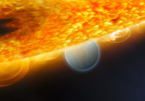
Up until now over 330 planets observed orbiting stars other than our Sun and, after next month, this total may start to increase rapidly as NASA launches its Kepler telescope to search for more “exoplanets”. So far, most exoplanets have been gas giants like Jupiter, but one of Kepler’s goals is to find Earth-sized planets at a “habitable” distance from their parent stars.

The question is, once astrophysicists start to see these Earth-like planets, how will we know if they are harbouring life?

(more…)

Big gains for physics as Obama signs stimulus bill

Science fared well in the $787bn package to stimulate the US economy that President Barack Obama signed into law today. The “recovery and reinvestment bill” includes $21.5bn for research and development (R&D), the bulk of which — some $18bn — will go directly to researchers. The remaining $3.5bn is allocated for facilities and equipment.

Politicians have been bickering over the bill since it was first unveiled on 15 January. American legislation takes a circuitous course on its way to the president. Typically, the House of Representatives and the Senate approve different versions of a bill, and then appoint negotiators to agree on compromise legislation that both houses must approve again before sending it to the president.

These prudent investments lay the necessary foundation for long-term economic growth and prosperity for our country Cherry Murray, American Physical Society

The $838bn Senate bill on 10 February included significantly less funding for physical science than the $825bn House bill on 29 January. Even though the Senate bill may have higher priority, most of the cuts to the physical sciences were reversed in the final $787bn bill agreed on 14 February. Indeed, physicists have welcomed the $21.5bn for science, with more than $10 bn of it going to government agencies responsible for funding the physical sciences.

NSF is a winner

The National Science Foundation (NSF) will receive $3bn in stimulus funding on top of its $6bn budget for 2009. This will include $1bn for research infrastructure and construction and $2bn for “other research and related activities.”

The DOE’s Office of Science, meanwhile, will get $1.6bn in funding beyond its 2009 budget of $4.0bn. Two other DOE programmes: energy efficiency and renewables, and fossil energy will receive $2.5bn and $1.0bn respectively, which is almost twice as much as their 2009 budget allocations of $1.2bn and $576m.

With a budget of $737m for this year, the National Institute of Standards and Technology will receive an extra $580 m, of which $360 m will go on building research facilities. NASA will receive an extra $1.1bn beyond its current budget of $17.2bn with $400m going towards its science and exploration programme.

The good news is that there is a lot of money for infrastructure. The big challenge is how to spend it Kei Koizumi, American Association for the Advancement of Science

“The surprise is how much money there is for science in the final bill,” says Kei Koizumi, budget analyst at the American Association for the Advancement of Science. “The good news is that there is a lot of money for infrastructure. The big challenge is how to spend it.”

“These critical investments will not only benefit American science and innovation, but they will put thousands of Americans back to work through construction and manufacturing projects,” American Physical Society president Cherry Murray said in a statement. “Furthermore, these prudent investments lay the necessary foundation for long-term economic growth and prosperity for our country.”

The fresh funding has implications for US science beyond the current financial year. It puts back on track the goal of doubling federal government support for physical science — an ambition of the America COMPETES Act of 2007 that had fallen behind schedule.

Further evidence of the Obama administration’s ambitions for science will become clear later this month, with the release of its revised budget for the 2009 financial year, which started on the 1st of October last year.

Type-1.5 superconductor shows its stripes

Anyone who has taken a condensed-matter physics course knows that superconductors can be classified neatly into type-1 or type-2 according to how they behave in an applied magnetic field. But now physicists in Belgium and Switzerland have found that at least one material — magnesium diboride — combines the characteristics of both types, leading the team to claim discovery of a complete new kind of superconductor called “type-1.5”.

Most conventional low-temperature superconductors are of the type-1 variety, which means that a magnetic field cannot usually penetrate the material. A magnetic field can, however, penetrate type-2 superconductors by creating tiny quantized vortices that grow in number as the field strength is increased. The field passes through a whisker of normal material at the centre of each vortex. The vortices repel each other, and as their numbers grow they form a vortex lattice.

This distinction is not quite so clear because under certain special conditions, field lines can penetrate type–1 materials. If the temperature of the material is changed rapidly (quenched) vortices will form but will attract each other and vanish upon collision. Also, when very thin samples of type-1 superconductors are exposed to a magnetic field, alternating stripes of superconducting and normal material can occur.

Behaving both ways

Now, Victor Moshchalkov and colleagues at the Catholic University of Leuven and the Swiss Federal Institute of Technology in Zürich are the first to show that the vortices in single-crystal samples of magnesium diboride (MgB2) behave in both ways. They have dubbed the material a type-1.5 superconductor because its vortices appear to repel each other over short distances and attract each other over longer distances (arXiv:0902.0997).

The result is a collection of vortices and non-superconducting regions that are organized into striped and gossamer patterns — depending upon the temperature of the sample and the strength of the magnetic field. Moshchalkov told physicsworld.com the patterns are similar to those seen in some liquid crystals and polymer films, in which the constituent molecules have similar attractive and repulsive interactions.

Moshchalkov believes that the type-1.5 behaviour can be understood by thinking of the material as containing two nearly independent superconducting fluids, which interact such that superconducting electrons can flow from one fluid to another.

Interacting mixture

Two-fluid systems with vortices of this type of interaction were predicted in 2005 by Egor Babaev of the University of Massachusetts in the US who describes it as comprising an “interacting mixture of two superconducting components which simultaneously shows properties of type-1 and type-2 superconductivity”.

Moshchalkov believes that there are more type-1.5 materials out there to be found, in addition to magnesium diboride, which was first found to be a superconductor in 2001. In particular, he believes that some of the iron-based superconductors discovered last year are prime candidates. He also believes that “artificial” type-1.5 materials can be made by placing a thin layer of type-1 material onto a thin layer of type-2 — something that the team is currently investigating.

Babaev looks forward to further research into type-1.5 materials because it could uncover many more vortex patterns that have never been seen before — with the possibility of phase transitions between patterns as magnetic-field strength is changed. In addition, he says that the work will be of interest to astrophysicists, who have suggested that type-1.5 behaviour might also occur a superconducting state of protons that is believed to exist in neutron stars.

Copyright © 2026 by IOP Publishing Ltd and individual contributors